目录
IIC协议这里就不赘述了,网上很多,这里推荐两个,可以看看【接口时序】6、IIC总线的原理与Verilog实现 ,还有IIC协议原理以及主机、从机Verilog实现。
前者是对IIC协议详细介绍、以及主机发送,主机接收两种方式。后者,是在前者基础上做设计,讲的是主机、从机两种设计实例。关于IIC从机,网上例程较少,可以参考这个博主的。不过,这个博主的状态机写的很乱,也没什么注释,看了两天才搞明白Verilog描述的什么,如果有FPGA爱好者需要用到,又看不懂的,可以私信我:bumianzhe@126.com.
本程序参考芯路恒IIC设计,可以去他们官网下完整资料看看。
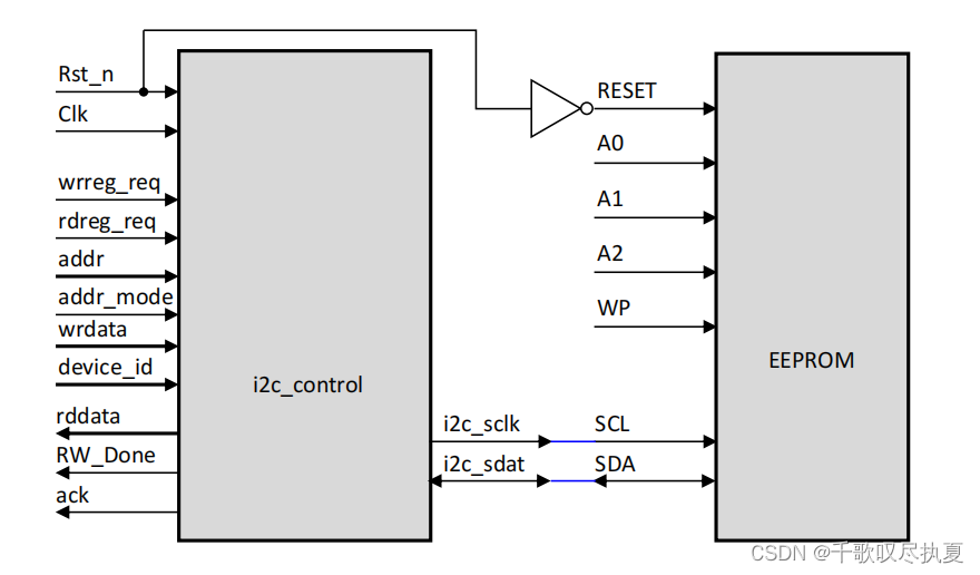
顶层模块:用来控制底层模块连续读写,包含了状态机
module i2c_control(
	Clk,
	Rst_n,

	wrreg_req,
	rdreg_req,
	addr,
	addr_mode,
	wrdata,
	rddata,
	device_id,
	RW_Done,

	ack,

	i2c_sclk,
	i2c_sdat
);

	input Clk;
	input Rst_n;

	input wrreg_req;
	input rdreg_req;
	input [15:0]addr;
	input addr_mode;
	input [7:0]wrdata;
	output reg[7:0]rddata;
	input [7:0]device_id;
	output reg RW_Done;

	output reg ack;

	output i2c_sclk;
	inout i2c_sdat;

	reg [5:0]Cmd;
	reg [7:0]Tx_DATA;
	wire Trans_Done;
	wire ack_o;
	reg Go;
	wire [15:0] reg_addr;

	assign reg_addr = addr_mode?addr:{addr[7:0],addr[15:8]};

	wire [7:0]Rx_DATA;

	localparam
		WR   = 6'b000001,   //写请求
		STA  = 6'b000010,   //起始位请求
		RD   = 6'b000100,   //读请求
		STO  = 6'b001000,   //停止位请求
		ACK  = 6'b010000,   //应答位请求
		NACK = 6'b100000;   //无应答请求

	i2c_bit_shift i2c_bit_shift(
		.Clk(Clk),
		.Rst_n(Rst_n),
		.Cmd(Cmd),
		.Go(Go),
		.Rx_DATA(Rx_DATA),
		.Tx_DATA(Tx_DATA),
		.Trans_Done(Trans_Done),
		.ack_o(ack_o),
		.i2c_sclk(i2c_sclk),
		.i2c_sdat(i2c_sdat)
	);

	reg [6:0]state;
	reg [7:0]cnt;

	localparam
		IDLE         = 7'b0000001,   //空闲状态
		WR_REG       = 7'b0000010,   //写寄存器状态
		WAIT_WR_DONE = 7'b0000100,   //等待写寄存器完成状态
		WR_REG_DONE  = 7'b0001000,   //写寄存器完成状态
		RD_REG       = 7'b0010000,   //读寄存器状态
		WAIT_RD_DONE = 7'b0100000,   //等待读寄存器完成状态
		RD_REG_DONE  = 7'b1000000;   //读寄存器完成状态

	always@(posedge Clk or negedge Rst_n)
	if(!Rst_n)begin
		Cmd <= 6'd0;
		Tx_DATA <= 8'd0;
		Go <= 1'b0;
		rddata <= 0;
		state <= IDLE;
		ack <= 0;
	end
	else begin
		case(state)
			IDLE:
				begin
					cnt <= 0;
					ack <= 0;
					RW_Done <= 1'b0;
					if(wrreg_req)
						state <= WR_REG;
					else if(rdreg_req)
						state <= RD_REG;
					else
						state <= IDLE;
				end

			WR_REG:
				begin
					state <= WAIT_WR_DONE;
					case(cnt)
						0:write_byte(WR | STA, device_id);
						1:write_byte(WR, reg_addr[15:8]);
						2:write_byte(WR, reg_addr[7:0]);
						3:write_byte(WR | STO, wrdata);
						default:;
					endcase
				end

			WAIT_WR_DONE:
				begin
					Go <= 1'b0;
					if(Trans_Done)begin
						ack <= ack | ack_o;
						case(cnt)
							0: begin cnt <= 1; state <= WR_REG;end
							1:
								begin
									state <= WR_REG;
									if(addr_mode)
										cnt <= 2;
									else
										cnt <= 3;
								end

							2: begin
									cnt <= 3;
									state <= WR_REG;
								end
							3:state <= WR_REG_DONE;
							default:state <= IDLE;
						endcase
					end
				end

			WR_REG_DONE:
				begin
					RW_Done <= 1'b1;
					state <= IDLE;
				end

			RD_REG:
				begin
					state <= WAIT_RD_DONE;
					case(cnt)
						0:write_byte(WR | STA, device_id);
						1:write_byte(WR, reg_addr[15:8]);
						2:write_byte(WR, reg_addr[7:0]);
						3:write_byte(WR | STA, device_id | 8'd1);
						4:read_byte(RD | NACK | STO);
						default:;
					endcase
				end

			WAIT_RD_DONE:
				begin
					Go <= 1'b0;
					if(Trans_Done)begin
						if(cnt <= 3)
							ack <= ack | ack_o;
						case(cnt)
							0: begin cnt <= 1; state <= RD_REG;end
							1:
								begin
									state <= RD_REG;
									if(addr_mode)
										cnt <= 2;
									else
										cnt <= 3;
								end

							2: begin
									cnt <= 3;
									state <= RD_REG;
								end
							3:begin
									cnt <= 4;
									state <= RD_REG;
								end
							4:state <= RD_REG_DONE;
							default:state <= IDLE;
						endcase
					end
				end

			RD_REG_DONE:
				begin
					RW_Done <= 1'b1;
					rddata <= Rx_DATA;
					state <= IDLE;
				end
			default:state <= IDLE;
		endcase
	end

	task read_byte;
		input [5:0]Ctrl_Cmd;
		begin
			Cmd <= Ctrl_Cmd;
			Go <= 1'b1;
		end
	endtask

	task write_byte;
		input [5:0]Ctrl_Cmd;
		input [7:0]Wr_Byte_Data;
		begin
			Cmd <= Ctrl_Cmd;
			Tx_DATA <= Wr_Byte_Data;
			Go <= 1'b1;
		end
	endtask

endmodule
子模块:单字节读写操作
module i2c_bit_shift(
	Clk,
	Rst_n,

	Cmd,
	Go,
	Rx_DATA,
	Tx_DATA,
	Trans_Done,
	ack_o,
	i2c_sclk,
	i2c_sdat
);
	input Clk;
	input Rst_n;

	input [5:0]Cmd;
	input Go;
	output reg[7:0]Rx_DATA;
	input [7:0]Tx_DATA;
	output reg Trans_Done;
	output reg ack_o;
	output reg i2c_sclk;
	inout i2c_sdat;

	reg i2c_sdat_o;

	//系统时钟采用50MHz
	parameter SYS_CLOCK = 50_000_000;
	//SCL总线时钟采用400kHz
	parameter SCL_CLOCK = 400_000;
	//产生时钟SCL计数器最大值
	localparam SCL_CNT_M = SYS_CLOCK/SCL_CLOCK/4 - 1;

	reg i2c_sdat_oe;

	localparam
		WR   = 6'b000001,   //写请求
		STA  = 6'b000010,   //起始位请求
		RD   = 6'b000100,   //读请求
		STO  = 6'b001000,   //停止位请求
		ACK  = 6'b010000,   //应答位请求
		NACK = 6'b100000;   //无应答请求

	reg [19:0]div_cnt;
	reg en_div_cnt;
	always@(posedge Clk or negedge Rst_n)
	if(!Rst_n)
		div_cnt <= 20'd0;
	else if(en_div_cnt)begin
		if(div_cnt < SCL_CNT_M)
			div_cnt <= div_cnt + 1'b1;
		else
			div_cnt <= 0;
	end
	else
		div_cnt <= 0;

	wire sclk_plus = div_cnt == SCL_CNT_M;

	//assign i2c_sdat = i2c_sdat_oe?i2c_sdat_o:1'bz;
	assign i2c_sdat = !i2c_sdat_o && i2c_sdat_oe ? 1'b0:1'bz;

	reg [7:0]state;

	localparam
		IDLE      = 8'b00000001,   //空闲状态
		GEN_STA   = 8'b00000010,   //产生起始信号
		WR_DATA   = 8'b00000100,   //写数据状态
		RD_DATA   = 8'b00001000,   //读数据状态
		CHECK_ACK = 8'b00010000,   //检测应答状态
		GEN_ACK   = 8'b00100000,   //产生应答状态
		GEN_STO   = 8'b01000000;   //产生停止信号

	reg [4:0]cnt;

	always@(posedge Clk or negedge Rst_n)
	if(!Rst_n)begin
		Rx_DATA <= 0;
		i2c_sdat_oe <= 1'd0;
		en_div_cnt <= 1'b0;
		i2c_sdat_o <= 1'd1;
		Trans_Done <= 1'b0;
		ack_o <= 0;
		state <= IDLE;
		cnt <= 0;
	end
	else begin
		case(state)
			IDLE:
				begin
					Trans_Done <= 1'b0;
					i2c_sdat_oe <= 1'd1;
					if(Go)begin
						en_div_cnt <= 1'b1;
						if(Cmd & STA)
							state <= GEN_STA;
						else if(Cmd & WR)
							state <= WR_DATA;
						else if(Cmd & RD)
							state <= RD_DATA;
						else
							state <= IDLE;
					end
					else begin
						en_div_cnt <= 1'b0;
						state <= IDLE;
					end
				end

			GEN_STA:
				begin
					if(sclk_plus)begin
						if(cnt == 3)
							cnt <= 0;
						else
							cnt <= cnt + 1'b1;
						case(cnt)
							0:begin i2c_sdat_o <= 1; i2c_sdat_oe <= 1'd1;end
							1:begin i2c_sclk <= 1;end
							2:begin i2c_sdat_o <= 0; i2c_sclk <= 1;end
							3:begin i2c_sclk <= 0;end
							default:begin i2c_sdat_o <= 1; i2c_sclk <= 1;end
						endcase
						if(cnt == 3)begin
							if(Cmd & WR)
								state <= WR_DATA;
							else if(Cmd & RD)
								state <= RD_DATA;
						end
					end
				end

			WR_DATA:
				begin
					if(sclk_plus)begin
						if(cnt == 31)
							cnt <= 0;
						else
							cnt <= cnt + 1'b1;
						case(cnt)
							0,4,8,12,16,20,24,28:begin i2c_sdat_o <= Tx_DATA[7-cnt[4:2]]; i2c_sdat_oe <= 1'd1;end	//set data;
							1,5,9,13,17,21,25,29:begin i2c_sclk <= 1;end	//sclk posedge
							2,6,10,14,18,22,26,30:begin i2c_sclk <= 1;end	//sclk keep high
							3,7,11,15,19,23,27,31:begin i2c_sclk <= 0;end	//sclk negedge
/*
							0 :begin i2c_sdat_o <= Tx_DATA[7];end
							1 :begin i2c_sclk <= 1;end	//sclk posedge
							2 :begin i2c_sclk <= 1;end	//sclk keep high
							3 :begin i2c_sclk <= 0;end	//sclk negedge

							4 :begin i2c_sdat_o <= Tx_DATA[6];end
							5 :begin i2c_sclk <= 1;end	//sclk posedge
							6 :begin i2c_sclk <= 1;end	//sclk keep high
							7 :begin i2c_sclk <= 0;end	//sclk negedge

							8 :begin i2c_sdat_o <= Tx_DATA[5];end
							9 :begin i2c_sclk <= 1;end	//sclk posedge
							10:begin i2c_sclk <= 1;end	//sclk keep high
							11:begin i2c_sclk <= 0;end	//sclk negedge

							12:begin i2c_sdat_o <= Tx_DATA[4];end
							13:begin i2c_sclk <= 1;end	//sclk posedge
							14:begin i2c_sclk <= 1;end	//sclk keep high
							15:begin i2c_sclk <= 0;end	//sclk negedge

							16:begin i2c_sdat_o <= Tx_DATA[3];end
							17:begin i2c_sclk <= 1;end	//sclk posedge
							18:begin i2c_sclk <= 1;end	//sclk keep high
							19:begin i2c_sclk <= 0;end	//sclk negedge

							20:begin i2c_sdat_o <= Tx_DATA[2];end
							21:begin i2c_sclk <= 1;end	//sclk posedge
							22:begin i2c_sclk <= 1;end	//sclk keep high
							23:begin i2c_sclk <= 0;end	//sclk negedge

							24:begin i2c_sdat_o <= Tx_DATA[1];end
							25:begin i2c_sclk <= 1;end	//sclk posedge
							26:begin i2c_sclk <= 1;end	//sclk keep high
							27:begin i2c_sclk <= 0;end	//sclk negedge

							28:begin i2c_sdat_o <= Tx_DATA[0];end
							29:begin i2c_sclk <= 1;end	//sclk posedge
							30:begin i2c_sclk <= 1;end	//sclk keep high
							31:begin i2c_sclk <= 0;end	//sclk negedge
*/
							default:begin i2c_sdat_o <= 1; i2c_sclk <= 1;end
						endcase
						if(cnt == 31)begin
							state <= CHECK_ACK;
						end
					end
				end

			RD_DATA:
				begin
					if(sclk_plus)begin
						if(cnt == 31)
							cnt <= 0;
						else
							cnt <= cnt + 1'b1;
						case(cnt)
							0,4,8,12,16,20,24,28:begin i2c_sdat_oe <= 1'd0; i2c_sclk <= 0;end	//set data;
							1,5,9,13,17,21,25,29:begin i2c_sclk <= 1;end	//sclk posedge
							2,6,10,14,18,22,26,30:begin i2c_sclk <= 1; Rx_DATA <= {Rx_DATA[6:0],i2c_sdat};end	//sclk keep high
							3,7,11,15,19,23,27,31:begin i2c_sclk <= 0;end	//sclk negedge
							default:begin i2c_sdat_o <= 1; i2c_sclk <= 1;end
						endcase
						if(cnt == 31)begin
							state <= GEN_ACK;
						end
					end
				end

			CHECK_ACK:
				begin
					if(sclk_plus)begin
						if(cnt == 3)
							cnt <= 0;
						else
							cnt <= cnt + 1'b1;
						case(cnt)
							0:begin i2c_sdat_oe <= 1'd0; i2c_sclk <= 0;end
							1:begin i2c_sclk <= 1;end
							2:begin ack_o <= i2c_sdat; i2c_sclk <= 1;end
							3:begin i2c_sclk <= 0;end
							default:begin i2c_sdat_o <= 1; i2c_sclk <= 1;end
						endcase
						if(cnt == 3)begin
							if(Cmd & STO)
								state <= GEN_STO;
							else begin
								state <= IDLE;
								Trans_Done <= 1'b1;
							end
						end
					end
				end

			GEN_ACK:
				begin
					if(sclk_plus)begin
						if(cnt == 3)
							cnt <= 0;
						else
							cnt <= cnt + 1'b1;
						case(cnt)
							0:begin
									i2c_sdat_oe <= 1'd1;
									i2c_sclk <= 0;
									if(Cmd & ACK)
										i2c_sdat_o <= 1'b0;
									else if(Cmd & NACK)
										i2c_sdat_o <= 1'b1;
								end
							1:begin i2c_sclk <= 1;end
							2:begin i2c_sclk <= 1;end
							3:begin i2c_sclk <= 0;end
							default:begin i2c_sdat_o <= 1; i2c_sclk <= 1;end
						endcase
						if(cnt == 3)begin
							if(Cmd & STO)
								state <= GEN_STO;
							else begin
								state <= IDLE;
								Trans_Done <= 1'b1;
							end
						end
					end
				end

			GEN_STO:
				begin
					if(sclk_plus)begin
						if(cnt == 3)
							cnt <= 0;
						else
							cnt <= cnt + 1'b1;
						case(cnt)
							0:begin i2c_sdat_o <= 0; i2c_sdat_oe <= 1'd1;end
							1:begin i2c_sclk <= 1;end
							2:begin i2c_sdat_o <= 1; i2c_sclk <= 1;end
							3:begin i2c_sclk <= 1;end
							default:begin i2c_sdat_o <= 1; i2c_sclk <= 1;end
						endcase
						if(cnt == 3)begin
							Trans_Done <= 1'b1;
							state <= IDLE;
						end
					end
				end
			default:state <= IDLE;
		endcase
	end

endmodule
镁 光 官 网 提 供 的 EEPROM 仿 真 模 型 , 具 体 下 载 网 址 为 :
http://ww1.microchip.com/downloads/en/DeviceDoc/24xx04_Verilog_Model.zip
1、本次使用的是1 字节寄存器地址段的 24LC04B 仿真模型,进行验证
// *******************************************************************************************************
// **                                                                           			**
// **   24LC04B.v - Microchip 24LC04B 4K-BIT I2C SERIAL EEPROM (VCC = +2.5V TO +5.5V)			**
// **                                                                           			**
// *******************************************************************************************************
// **                                                                           			**
// **			This information is distributed under license from Young Engineering.		**
// **                              COPYRIGHT (c) 2003 YOUNG ENGINEERING              			**
// **                                      ALL RIGHTS RESERVED                         			**
// **                                                                           			**
// **                                                                                                   **
// **   Young Engineering provides design expertise for the digital world                               **
// **   Started in 1990, Young Engineering offers products and services for your electronic design      **
// **   project.  We have the expertise in PCB, FPGA, ASIC, firmware, and software design.              **
// **   From concept to prototype to production, we can help you.                                       **
// **													**
// **	http://www.young-engineering.com/								**
// **													**
// *******************************************************************************************************
// **	This information is provided to you for your convenience and use with Microchip products only.  **
// **	Microchip disclaims all liability arising from this information and its use.  			**
// **													**
// **	THIS INFORMATION IS PROVIDED "AS IS." MICROCHIP MAKES NO REPRESENTATION OR WARRANTIES OF 	**
// **	ANY KIND WHETHER EXPRESS OR IMPLIED, WRITTEN OR ORAL, STATUTORY OR OTHERWISE, RELATED TO 	**
// **	THE INFORMATION PROVIDED TO YOU, INCLUDING BUT NOT LIMITED TO ITS CONDITION, QUALITY, 		**
// **	PERFORMANCE, MERCHANTABILITY, NON-INFRINGEMENT, OR FITNESS FOR PURPOSE.  			**
// **	MICROCHIP IS NOT LIABLE, UNDER ANY CIRCUMSTANCES, FOR SPECIAL, INCIDENTAL OR CONSEQUENTIAL 	**
// **	DAMAGES, FOR ANY REASON WHATSOEVER.								**
// **													**
// **	It is your responsibility to ensure that your application meets with your specifications.	**
// **													**
// *******************************************************************************************************
// **   Revision       : 1.3                                                    			**
// **   Modified Date  : 12/04/2006	                                            			**
// **   Revision History:                                                       			**
// **                                                                           			**
// **   02/01/2003:  Initial design                                             			**
// **   07/19/2004:  Fixed the timing checks and the open-drain modeling for SDA.			**
// **   01/06/2006:  Changed the legal information in the header					**
// **   12/04/2006:  Corrected timing checks to reference proper clock edges				**
// **                Added timing check for Tbuf (bus free time)					**
// **                                                                           			**
// *******************************************************************************************************
// **                                       TABLE OF CONTENTS                          			**
// *******************************************************************************************************
// **---------------------------------------------------------------------------------------------------**
// **   DECLARATIONS                                                          				**
// **---------------------------------------------------------------------------------------------------**
// **---------------------------------------------------------------------------------------------------**
// **   INITIALIZATION                                              					**
// **---------------------------------------------------------------------------------------------------**
// **---------------------------------------------------------------------------------------------------**
// **   CORE LOGIC                                                  					**
// **---------------------------------------------------------------------------------------------------**
// **   1.01:  START Bit Detection									**
// **   1.02:  STOP Bit Detection									**
// **   1.03:  Input Shift Register									**
// **   1.04:  Input Bit Counter									**
// **   1.05:  Control Byte Register									**
// **   1.06:  Byte Address Register									**
// **   1.07:  Write Data Buffer									**
// **   1.08:  Acknowledge Generator									**
// **   1.09:  Acknowledge Detect									**
// **   1.10:  Write Cycle Timer									**
// **   1.11:  Write Cycle Processor									**
// **   1.12:  Read Data Multiplexor									**
// **   1.13:  Read Data Processor									**
// **   1.14:  SDA Data I/O Buffer									**
// **                                                                           			**
// **---------------------------------------------------------------------------------------------------**
// **   DEBUG LOGIC                                                  					**
// **---------------------------------------------------------------------------------------------------**
// **   2.01:  Memory Data Bytes									**
// **   2.02:  Write Data Buffer									**
// **                                                                           			**
// **---------------------------------------------------------------------------------------------------**
// **   TIMING CHECKS                                                     				**
// **---------------------------------------------------------------------------------------------------**
// **                                                                           			**
// *******************************************************************************************************


`timescale 1ns/10ps

module M24LC04B (A0, A1, A2, WP, SDA, SCL, RESET);

   input 		A0;				// unconnected pin
   input 		A1;				// unconnected pin
   input 		A2;				// unconnected pin

   input		WP;				// write protect pin

   inout		SDA;		  // serial data I/O
   input		SCL;		  // serial data clock

   input		RESET;	  // system reset


// *******************************************************************************************************
// **   DECLARATIONS                                                            			**
// *******************************************************************************************************

   reg			      SDA_DO;				          // serial data - output
   reg            SDA_OE;				          // serial data - output enable

   wire			      SDA_DriveEnable;    		// serial data output enable
   reg			      SDA_DriveEnableDlyd;		// serial data output enable - delayed

   wire [02:00]   ChipAddress;            // hardwired chip address

   reg	[03:00]		BitCounter;		        	// serial bit counter

   reg			      START_Rcvd;		        	// START bit received flag
   reg			      STOP_Rcvd;		        	// STOP bit received flag
   reg			      CTRL_Rcvd;		         	// control byte received flag
   reg			      ADDR_Rcvd;		        	// byte address received flag
   reg			      MACK_Rcvd;		         	// master acknowledge received flag

   reg			      WrCycle;			          // memory write cycle
   reg			      RdCycle;			          // memory read cycle

   reg	[07:00]		ShiftRegister;	    		// input data shift register

   reg  [07:00]		ControlByte;		      	// control byte register
   wire			      BlockSelect;		      	// memory block select
   wire			      RdWrBit;			          // read/write control bit

   reg	[08:00]		StartAddress;			      // memory access starting address
   reg	[03:00]		PageAddress;			      // memory page address

   reg	[07:00]		WrDataByte [0:15];	  	// memory write data buffer
   wire	[07:00]		RdDataByte;			        // memory read data

   reg	[15:00]		WrCounter;			        // write buffer counter

   reg	[03:00]		WrPointer;			        // write buffer pointer
   reg	[08:00]		RdPointer;			        // read address pointer

   reg			      WriteActive;			      // memory write cycle active

   reg	[07:00]		MemoryBlock0 [0:255];		// EEPROM data memory array
   reg	[07:00]		MemoryBlock1 [0:255];		// EEPROM data memory array

   integer		    LoopIndex;		        	// iterative loop index

   integer 		    tAA;			            	// timing parameter
   integer 		    tWC;			            	// timing parameter


// *******************************************************************************************************
// **   INITIALIZATION                                                         				**
// *******************************************************************************************************

   initial tAA = 900;                                   // SCL to SDA output delay
   initial tWC = 5000000;                               // memory write cycle time

   initial begin
      SDA_DO = 0;
      SDA_OE = 0;
   end

   initial begin
      START_Rcvd = 0;
      STOP_Rcvd  = 0;
      CTRL_Rcvd  = 0;
      ADDR_Rcvd  = 0;
      MACK_Rcvd  = 0;
   end

   initial begin
      BitCounter  = 0;
      ControlByte = 0;
   end

   initial begin
      WrCycle = 0;
      RdCycle = 0;

      WriteActive = 0;
   end

   assign ChipAddress = {A2,A1,A0};

// *******************************************************************************************************
// **   CORE LOGIC                                                    					**
// *******************************************************************************************************
// -------------------------------------------------------------------------------------------------------
//      1.01:  START Bit Detection
// -------------------------------------------------------------------------------------------------------

   always @(negedge SDA) begin
      if (SCL == 1) begin
         START_Rcvd <= 1;
         STOP_Rcvd  <= 0;
         CTRL_Rcvd  <= 0;
         ADDR_Rcvd  <= 0;
         MACK_Rcvd  <= 0;

         WrCycle <= #1 0;
         RdCycle <= #1 0;

         BitCounter <= 0;
      end
   end

// -------------------------------------------------------------------------------------------------------
//      1.02:  STOP Bit Detection
// -------------------------------------------------------------------------------------------------------

   always @(posedge SDA) begin
      if (SCL == 1) begin
         START_Rcvd <= 0;
         STOP_Rcvd  <= 1;
         CTRL_Rcvd  <= 0;
         ADDR_Rcvd  <= 0;
         MACK_Rcvd  <= 0;

         WrCycle <= #1 0;
         RdCycle <= #1 0;

         BitCounter <= 10;
      end
   end

// -------------------------------------------------------------------------------------------------------
//      1.03:  Input Shift Register
// -------------------------------------------------------------------------------------------------------

   always @(posedge SCL) begin
      ShiftRegister[00] <= SDA;
      ShiftRegister[01] <= ShiftRegister[00];
      ShiftRegister[02] <= ShiftRegister[01];
      ShiftRegister[03] <= ShiftRegister[02];
      ShiftRegister[04] <= ShiftRegister[03];
      ShiftRegister[05] <= ShiftRegister[04];
      ShiftRegister[06] <= ShiftRegister[05];
      ShiftRegister[07] <= ShiftRegister[06];
   end

// -------------------------------------------------------------------------------------------------------
//      1.04:  Input Bit Counter
// -------------------------------------------------------------------------------------------------------

   always @(posedge SCL) begin
      if (BitCounter < 10) BitCounter <= BitCounter + 1;
   end

// -------------------------------------------------------------------------------------------------------
//      1.05:  Control Byte Register
// -------------------------------------------------------------------------------------------------------

   always @(negedge SCL) begin
      if (START_Rcvd & (BitCounter == 8)) begin
         if (!WriteActive & (ShiftRegister[07:01] == {4'b1010,ChipAddress[02:00]})) begin
            if (ShiftRegister[00] == 0) WrCycle <= 1;
            if (ShiftRegister[00] == 1) RdCycle <= 1;

            ControlByte <= ShiftRegister[07:00];

            CTRL_Rcvd <= 1;
         end

         START_Rcvd <= 0;
      end
   end

   assign BlockSelect = ControlByte[01];
   assign RdWrBit     = ControlByte[00];

// -------------------------------------------------------------------------------------------------------
//      1.06:  Byte Address Register
// -------------------------------------------------------------------------------------------------------

   always @(negedge SCL) begin
      if (CTRL_Rcvd & (BitCounter == 8)) begin
         if (RdWrBit == 0) begin
            StartAddress <= {BlockSelect,ShiftRegister[07:00]};
            RdPointer    <= {BlockSelect,ShiftRegister[07:00]};

            ADDR_Rcvd <= 1;
         end

         WrCounter <= 0;
         WrPointer <= 0;

         CTRL_Rcvd <= 0;
      end
   end

// -------------------------------------------------------------------------------------------------------
//      1.07:  Write Data Buffer
// -------------------------------------------------------------------------------------------------------

   always @(negedge SCL) begin
      if (ADDR_Rcvd & (BitCounter == 8)) begin
         if ((WP == 0) & (RdWrBit == 0)) begin
            WrDataByte[WrPointer] <= ShiftRegister[07:00];

            WrCounter <= WrCounter + 1;
            WrPointer <= WrPointer + 1;
         end
      end
   end

// -------------------------------------------------------------------------------------------------------
//      1.08:  Acknowledge Generator
// -------------------------------------------------------------------------------------------------------

   always @(negedge SCL) begin
      if (!WriteActive) begin
         if (BitCounter == 8) begin
            if (WrCycle | (START_Rcvd & (ShiftRegister[07:01] == {4'b1010,ChipAddress[02:00]}))) begin
               SDA_DO <= 0;
               SDA_OE <= 1;
            end
         end
         if (BitCounter == 9) begin
            BitCounter <= 0;

            if (!RdCycle) begin
               SDA_DO <= 0;
               SDA_OE <= 0;
            end
         end
      end
   end

// -------------------------------------------------------------------------------------------------------
//      1.09:  Acknowledge Detect
// -------------------------------------------------------------------------------------------------------

   always @(posedge SCL) begin
      if (RdCycle & (BitCounter == 8)) begin
         if ((SDA == 0) & (SDA_OE == 0)) MACK_Rcvd <= 1;
      end
   end

   always @(negedge SCL) MACK_Rcvd <= 0;

// -------------------------------------------------------------------------------------------------------
//      1.10:  Write Cycle Timer
// -------------------------------------------------------------------------------------------------------

   always @(posedge STOP_Rcvd) begin
      if (WrCycle & (WP == 0) & (WrCounter > 0)) begin
         WriteActive = 1;
         #(tWC);
         WriteActive = 0;
      end
   end

   always @(posedge STOP_Rcvd) begin
      #(1.0);
      STOP_Rcvd = 0;
   end

// -------------------------------------------------------------------------------------------------------
//      1.11:  Write Cycle Processor
// -------------------------------------------------------------------------------------------------------

   always @(negedge WriteActive) begin
      for (LoopIndex = 0; LoopIndex < WrCounter; LoopIndex = LoopIndex + 1) begin
         if (StartAddress[08] == 0) begin
            PageAddress = StartAddress[03:00] + LoopIndex;

            MemoryBlock0[{StartAddress[07:04],PageAddress[03:00]}] = WrDataByte[LoopIndex[03:00]];
         end
         if (StartAddress[08] == 1) begin
            PageAddress = StartAddress[03:00] + LoopIndex;

            MemoryBlock1[{StartAddress[07:04],PageAddress[03:00]}] = WrDataByte[LoopIndex[03:00]];
         end
      end
   end

// -------------------------------------------------------------------------------------------------------
//      1.12:  Read Data Multiplexor
// -------------------------------------------------------------------------------------------------------

   always @(negedge SCL) begin
      if (BitCounter == 8) begin
         if (WrCycle & ADDR_Rcvd) begin
            RdPointer <= StartAddress + WrPointer + 1;
         end
         if (RdCycle) begin
            RdPointer <= RdPointer + 1;
         end
      end
   end

   assign RdDataByte = RdPointer[08] ? MemoryBlock1[RdPointer[07:00]] : MemoryBlock0[RdPointer[07:00]];

// -------------------------------------------------------------------------------------------------------
//      1.13:  Read Data Processor
// -------------------------------------------------------------------------------------------------------

   always @(negedge SCL) begin
      if (RdCycle) begin
         if (BitCounter == 8) begin
            SDA_DO <= 0;
            SDA_OE <= 0;
         end
         else if (BitCounter == 9) begin
            SDA_DO <= RdDataByte[07];

            if (MACK_Rcvd) SDA_OE <= 1;
         end
         else begin
            SDA_DO <= RdDataByte[7-BitCounter];
         end
      end
   end

// -------------------------------------------------------------------------------------------------------
//      1.14:  SDA Data I/O Buffer
// -------------------------------------------------------------------------------------------------------

   bufif1 (SDA, 1'b0, SDA_DriveEnableDlyd);

   assign SDA_DriveEnable = !SDA_DO & SDA_OE;
   always @(SDA_DriveEnable) SDA_DriveEnableDlyd <= #(tAA) SDA_DriveEnable;


// *******************************************************************************************************
// **   DEBUG LOGIC                                                           				**
// *******************************************************************************************************
// -------------------------------------------------------------------------------------------------------
//      2.01:  Memory Data Bytes
// -------------------------------------------------------------------------------------------------------

   wire [07:00]	MemoryByte0_00 = MemoryBlock0[00];
   wire [07:00]	MemoryByte0_01 = MemoryBlock0[01];
   wire [07:00]	MemoryByte0_02 = MemoryBlock0[02];
   wire [07:00]	MemoryByte0_03 = MemoryBlock0[03];
   wire [07:00]	MemoryByte0_04 = MemoryBlock0[04];
   wire [07:00]	MemoryByte0_05 = MemoryBlock0[05];
   wire [07:00]	MemoryByte0_06 = MemoryBlock0[06];
   wire [07:00]	MemoryByte0_07 = MemoryBlock0[07];

   wire [07:00]	MemoryByte0_08 = MemoryBlock0[08];
   wire [07:00]	MemoryByte0_09 = MemoryBlock0[09];
   wire [07:00]	MemoryByte0_0A = MemoryBlock0[10];
   wire [07:00]	MemoryByte0_0B = MemoryBlock0[11];
   wire [07:00]	MemoryByte0_0C = MemoryBlock0[12];
   wire [07:00]	MemoryByte0_0D = MemoryBlock0[13];
   wire [07:00]	MemoryByte0_0E = MemoryBlock0[14];
   wire [07:00]	MemoryByte0_0F = MemoryBlock0[15];

   wire [07:00]	MemoryByte1_00 = MemoryBlock1[00];
   wire [07:00]	MemoryByte1_01 = MemoryBlock1[01];
   wire [07:00]	MemoryByte1_02 = MemoryBlock1[02];
   wire [07:00]	MemoryByte1_03 = MemoryBlock1[03];
   wire [07:00]	MemoryByte1_04 = MemoryBlock1[04];
   wire [07:00]	MemoryByte1_05 = MemoryBlock1[05];
   wire [07:00]	MemoryByte1_06 = MemoryBlock1[06];
   wire [07:00]	MemoryByte1_07 = MemoryBlock1[07];

   wire [07:00]	MemoryByte1_08 = MemoryBlock1[08];
   wire [07:00]	MemoryByte1_09 = MemoryBlock1[09];
   wire [07:00]	MemoryByte1_0A = MemoryBlock1[10];
   wire [07:00]	MemoryByte1_0B = MemoryBlock1[11];
   wire [07:00]	MemoryByte1_0C = MemoryBlock1[12];
   wire [07:00]	MemoryByte1_0D = MemoryBlock1[13];
   wire [07:00]	MemoryByte1_0E = MemoryBlock1[14];
   wire [07:00]	MemoryByte1_0F = MemoryBlock1[15];

// -------------------------------------------------------------------------------------------------------
//      2.02:  Write Data Buffer
// -------------------------------------------------------------------------------------------------------

   wire [07:00]	WriteData_0 = WrDataByte[00];
   wire [07:00]	WriteData_1 = WrDataByte[01];
   wire [07:00]	WriteData_2 = WrDataByte[02];
   wire [07:00]	WriteData_3 = WrDataByte[03];
   wire [07:00]	WriteData_4 = WrDataByte[04];
   wire [07:00]	WriteData_5 = WrDataByte[05];
   wire [07:00]	WriteData_6 = WrDataByte[06];
   wire [07:00]	WriteData_7 = WrDataByte[07];
   wire [07:00]	WriteData_8 = WrDataByte[08];
   wire [07:00]	WriteData_9 = WrDataByte[09];
   wire [07:00]	WriteData_A = WrDataByte[10];
   wire [07:00]	WriteData_B = WrDataByte[11];
   wire [07:00]	WriteData_C = WrDataByte[12];
   wire [07:00]	WriteData_D = WrDataByte[13];
   wire [07:00]	WriteData_E = WrDataByte[14];
   wire [07:00]	WriteData_F = WrDataByte[15];


// *******************************************************************************************************
// **   TIMING CHECKS                                                           			**
// *******************************************************************************************************

   wire TimingCheckEnable = (RESET == 0) & (SDA_OE == 0);

   specify
      specparam
         tHI = 600,                                     // SCL pulse width - high
         tLO = 1300,                                    // SCL pulse width - low
			   tSU_STA = 600,                                 // SCL to SDA setup time
         tHD_STA = 600,                                 // SCL to SDA hold time
         tSU_DAT = 100,                                 // SDA to SCL setup time
         tSU_STO = 600,                                 // SCL to SDA setup time
         tBUF = 1300;                                   // Bus free time

      $width (posedge SCL, tHI);
      $width (negedge SCL, tLO);

      $width (posedge SDA &&& SCL, tBUF);

      $setup (posedge SCL, negedge SDA &&& TimingCheckEnable, tSU_STA);
      $setup (SDA, posedge SCL &&& TimingCheckEnable, tSU_DAT);
      $setup (posedge SCL, posedge SDA &&& TimingCheckEnable, tSU_STO);

      $hold  (negedge SDA &&& TimingCheckEnable, negedge SCL, tHD_STA);
   endspecify

endmodule
2、M24LC64仿真模型供大家使用
// *******************************************************************************************************
// ** **
// ** 24LC64.v - Microchip 24LC64 64K-BIT I2C SERIAL EEPROM (VCC = +2.5V TO +5.5V) **
// ** **
// *******************************************************************************************************
// ** **
// ** This information is distributed under license from Young Engineering. **
// ** COPYRIGHT (c) 2009 YOUNG ENGINEERING **
// ** ALL RIGHTS RESERVED **
// ** **
// ** **
// ** Young Engineering provides design expertise for the digital world **
// ** Started in 1990, Young Engineering offers products and services for your electronic design **
// ** project. We have the expertise in PCB, FPGA, ASIC, firmware, and software design. **
// ** From concept to prototype to production, we can help you. **
// ** **
// ** http://www.young-engineering.com/ **
// ** **
// *******************************************************************************************************
// ** This information is provided to you for your convenience and use with Microchip products only. **
// ** Microchip disclaims all liability arising from this information and its use. **
// ** **
// ** THIS INFORMATION IS PROVIDED "AS IS." MICROCHIP MAKES NO REPRESENTATION OR WARRANTIES OF **
// ** ANY KIND WHETHER EXPRESS OR IMPLIED, WRITTEN OR ORAL, STATUTORY OR OTHERWISE, RELATED TO **
// ** THE INFORMATION PROVIDED TO YOU, INCLUDING BUT NOT LIMITED TO ITS CONDITION, QUALITY, **
// ** PERFORMANCE, MERCHANTABILITY, NON-INFRINGEMENT, OR FITNESS FOR PURPOSE. **
// ** MICROCHIP IS NOT LIABLE, UNDER ANY CIRCUMSTANCES, FOR SPECIAL, INCIDENTAL OR CONSEQUENTIAL **
// ** DAMAGES, FOR ANY REASON WHATSOEVER. **
// ** **
// ** It is your responsibility to ensure that your application meets with your specifications. **
// ** **
// *******************************************************************************************************
// ** Revision : 1.4 **
// ** Modified Date : 02/04/2009 **
// ** Revision History: **
// ** **
// ** 10/01/2003: Initial design **
// ** 07/19/2004: Fixed the timing checks and the open-drain modeling for SDA. **
// ** 01/06/2006: Changed the legal information in the header **
// ** 12/04/2006: Corrected timing checks to reference proper clock edges **
// ** Added timing check for Tbuf (bus free time) **
// ** Reduced memory blocks to single, monolithic array **
// ** 02/04/2009: Added timing checks for tSU_WP and tHD_WP **
// ** **
// *******************************************************************************************************
// ** TABLE OF CONTENTS **
// *******************************************************************************************************
// **---------------------------------------------------------------------------------------------------**
// ** DECLARATIONS **
// **---------------------------------------------------------------------------------------------------**
// **---------------------------------------------------------------------------------------------------**
// ** INITIALIZATION **
// **---------------------------------------------------------------------------------------------------**
// **---------------------------------------------------------------------------------------------------**
// ** CORE LOGIC **
// **---------------------------------------------------------------------------------------------------**
// ** 1.01: START Bit Detection **
// ** 1.02: STOP Bit Detection **
// ** 1.03: Input Shift Register **
// ** 1.04: Input Bit Counter **
// ** 1.05: Control Byte Register **
// ** 1.06: Byte Address Register **
// ** 1.07: Write Data Buffer **
// ** 1.08: Acknowledge Generator **
// ** 1.09: Acknowledge Detect **
// ** 1.10: Write Cycle Timer **
// ** 1.11: Write Cycle Processor **
// ** 1.12: Read Data Multiplexor **
// ** 1.13: Read Data Processor **
// ** 1.14: SDA Data I/O Buffer **
// ** **
// **---------------------------------------------------------------------------------------------------**
// ** DEBUG LOGIC **
// **---------------------------------------------------------------------------------------------------**
// ** 2.01: Memory Data Bytes **
// ** 2.02: Write Data Buffer **
// ** **
// **---------------------------------------------------------------------------------------------------**
// ** TIMING CHECKS **
// **---------------------------------------------------------------------------------------------------**
// ** **
// *******************************************************************************************************
`timescale 1ns/10ps
module M24LC64 (A0, A1, A2, WP, SDA, SCL, RESET);
input A0; // chip select bit
input A1; // chip select bit
input A2; // chip select bit
input WP; // write protect pin
inout SDA; // serial data I/O
input SCL; // serial data clock
input RESET; // system reset
// *******************************************************************************************************
// ** DECLARATIONS **
// *******************************************************************************************************
reg SDA_DO; // serial data - output
reg SDA_OE; // serial data - output enable
wire SDA_DriveEnable; // serial data output enable
reg SDA_DriveEnableDlyd; // serial data output enable - delayed
wire [02:00] ChipAddress; // hardwired chip address
reg [03:00] BitCounter; // serial bit counter
reg START_Rcvd; // START bit received flag
reg STOP_Rcvd; // STOP bit received flag
reg CTRL_Rcvd; // control byte received flag
reg ADHI_Rcvd; // byte address hi received flag
reg ADLO_Rcvd; // byte address lo received flag
reg MACK_Rcvd; // master acknowledge received flag
reg WrCycle; // memory write cycle
reg RdCycle; // memory read cycle
reg [07:00] ShiftRegister; // input data shift register
reg [07:00] ControlByte; // control byte register
wire RdWrBit; // read/write control bit
reg [12:00] StartAddress; // memory access starting address
reg [04:00] PageAddress; // memory page address
reg [07:00] WrDataByte [0:31]; // memory write data buffer
wire [07:00] RdDataByte; // memory read data
reg [15:00] WrCounter; // write buffer counter
reg [04:00] WrPointer; // write buffer pointer
reg [12:00] RdPointer; // read address pointer
reg WriteActive; // memory write cycle active
reg [07:00] MemoryBlock [0:8191]; // EEPROM data memory array
integer LoopIndex; // iterative loop index
integer tAA; // timing parameter
integer tWC; // timing parameter
// *******************************************************************************************************
// ** INITIALIZATION **
// *******************************************************************************************************
//----------------------------
//------写数据间隔改动----------
initial tAA = 900; // SCL to SDA output delay
initial tWC = 500; // memory write cycle time
// initial tAA = 900; // SCL to SDA output delay
// initial tWC = 5000000; // memory write cycle time
initial begin
SDA_DO = 0;
SDA_OE = 0;
end
initial begin
START_Rcvd = 0;
STOP_Rcvd = 0;
CTRL_Rcvd = 0;
ADHI_Rcvd = 0;
ADLO_Rcvd = 0;
MACK_Rcvd = 0;
end
initial begin
BitCounter = 0;
ControlByte = 0;
end
initial begin
WrCycle = 0;
RdCycle = 0;
WriteActive = 0;
end
assign ChipAddress = {A2,A1,A0};
// *******************************************************************************************************
// ** CORE LOGIC **
// *******************************************************************************************************
// -------------------------------------------------------------------------------------------------------
// 1.01: START Bit Detection
// -------------------------------------------------------------------------------------------------------
always @(negedge SDA) begin
if (SCL == 1) begin
START_Rcvd <= 1;
STOP_Rcvd <= 0;
CTRL_Rcvd <= 0;
ADHI_Rcvd <= 0;
ADLO_Rcvd <= 0;
MACK_Rcvd <= 0;
WrCycle <= #1 0;
RdCycle <= #1 0;
BitCounter <= 0;
end
end
// -------------------------------------------------------------------------------------------------------
// 1.02: STOP Bit Detection
// -------------------------------------------------------------------------------------------------------
always @(posedge SDA) begin
if (SCL == 1) begin
START_Rcvd <= 0;
STOP_Rcvd <= 1;
CTRL_Rcvd <= 0;
ADHI_Rcvd <= 0;
ADLO_Rcvd <= 0;
MACK_Rcvd <= 0;
WrCycle <= #1 0;
RdCycle <= #1 0;
BitCounter <= 10;
end
end
// -------------------------------------------------------------------------------------------------------
// 1.03: Input Shift Register
// -------------------------------------------------------------------------------------------------------
always @(posedge SCL) begin
ShiftRegister[00] <= SDA;
ShiftRegister[01] <= ShiftRegister[00];
ShiftRegister[02] <= ShiftRegister[01];
ShiftRegister[03] <= ShiftRegister[02];
ShiftRegister[04] <= ShiftRegister[03];
ShiftRegister[05] <= ShiftRegister[04];
ShiftRegister[06] <= ShiftRegister[05];
ShiftRegister[07] <= ShiftRegister[06];
end
// -------------------------------------------------------------------------------------------------------
// 1.04: Input Bit Counter
// -------------------------------------------------------------------------------------------------------
always @(posedge SCL) begin
if (BitCounter < 10) BitCounter <= BitCounter + 1;
end
// -------------------------------------------------------------------------------------------------------
// 1.05: Control Byte Register
// -------------------------------------------------------------------------------------------------------
always @(negedge SCL) begin
if (START_Rcvd & (BitCounter == 8)) begin
if (!WriteActive & (ShiftRegister[07:01] == {4'b1010,ChipAddress[02:00]})) begin
if (ShiftRegister[00] == 0) WrCycle <= 1;
if (ShiftRegister[00] == 1) RdCycle <= 1;
ControlByte <= ShiftRegister[07:00];
CTRL_Rcvd <= 1;
end
START_Rcvd <= 0;
end
end
assign RdWrBit = ControlByte[00];
// -------------------------------------------------------------------------------------------------------
// 1.06: Byte Address Register
// -------------------------------------------------------------------------------------------------------
always @(negedge SCL) begin
if (CTRL_Rcvd & (BitCounter == 8)) begin
if (RdWrBit == 0) begin
StartAddress[12:08] <= ShiftRegister[04:00];
RdPointer[12:08] <= ShiftRegister[04:00];
ADHI_Rcvd <= 1;
end
WrCounter <= 0;
WrPointer <= 0;
CTRL_Rcvd <= 0;
end
end
always @(negedge SCL) begin
if (ADHI_Rcvd & (BitCounter == 8)) begin
if (RdWrBit == 0) begin
StartAddress[07:00] <= ShiftRegister[07:00];
RdPointer[07:00] <= ShiftRegister[07:00];
ADLO_Rcvd <= 1;
end
WrCounter <= 0;
WrPointer <= 0;
ADHI_Rcvd <= 0;
end
end
// -------------------------------------------------------------------------------------------------------
// 1.07: Write Data Buffer
// -------------------------------------------------------------------------------------------------------
always @(negedge SCL) begin
if (ADLO_Rcvd & (BitCounter == 8)) begin
if (RdWrBit == 0) begin
WrDataByte[WrPointer] <= ShiftRegister[07:00];
WrCounter <= WrCounter + 1;
WrPointer <= WrPointer + 1;
end
end
end
// -------------------------------------------------------------------------------------------------------
// 1.08: Acknowledge Generator
// -------------------------------------------------------------------------------------------------------
always @(negedge SCL) begin
if (!WriteActive) begin
if (BitCounter == 8) begin
if (WrCycle | (START_Rcvd & (ShiftRegister[07:01] == {4'b1010,ChipAddress[02:00]}))) begin
SDA_DO <= 0;
SDA_OE <= 1;
end
end
if (BitCounter == 9) begin
BitCounter <= 0;
if (!RdCycle) begin
SDA_DO <= 0;
SDA_OE <= 0;
end
end
end
end
// -------------------------------------------------------------------------------------------------------
// 1.09: Acknowledge Detect
// -------------------------------------------------------------------------------------------------------
always @(posedge SCL) begin
if (RdCycle & (BitCounter == 8)) begin
if ((SDA == 0) & (SDA_OE == 0)) MACK_Rcvd <= 1;
end
end
always @(negedge SCL) MACK_Rcvd <= 0;
// -------------------------------------------------------------------------------------------------------
// 1.10: Write Cycle Timer
// -------------------------------------------------------------------------------------------------------
always @(posedge STOP_Rcvd) begin
if (WrCycle & (WP == 0) & (WrCounter > 0)) begin
WriteActive = 1;
#(tWC);
WriteActive = 0;
end
end
always @(posedge STOP_Rcvd) begin
#(1.0);
STOP_Rcvd = 0;
end
// -------------------------------------------------------------------------------------------------------
// 1.11: Write Cycle Processor
// -------------------------------------------------------------------------------------------------------
always @(negedge WriteActive) begin
for (LoopIndex = 0; LoopIndex < WrCounter; LoopIndex = LoopIndex + 1) begin
PageAddress = StartAddress[04:00] + LoopIndex;
MemoryBlock[{StartAddress[12:05],PageAddress[04:00]}] = WrDataByte[LoopIndex[04:00]];
end
end
// -------------------------------------------------------------------------------------------------------
// 1.12: Read Data Multiplexor
// -------------------------------------------------------------------------------------------------------
always @(negedge SCL) begin
if (BitCounter == 8) begin
if (WrCycle & ADLO_Rcvd) begin
RdPointer <= StartAddress + WrPointer + 1;
end
if (RdCycle) begin
RdPointer <= RdPointer + 1;
end
end
end
assign RdDataByte = MemoryBlock[RdPointer[12:00]];
// -------------------------------------------------------------------------------------------------------
// 1.13: Read Data Processor
// -------------------------------------------------------------------------------------------------------
always @(negedge SCL) begin
if (RdCycle) begin
if (BitCounter == 8) begin
SDA_DO <= 0;
SDA_OE <= 0;
end
else if (BitCounter == 9) begin
SDA_DO <= RdDataByte[07];
if (MACK_Rcvd) SDA_OE <= 1;
end
else begin
SDA_DO <= RdDataByte[7-BitCounter];
end
end
end
// -------------------------------------------------------------------------------------------------------
// 1.14: SDA Data I/O Buffer
// -------------------------------------------------------------------------------------------------------
bufif1 (SDA, 1'b0, SDA_DriveEnableDlyd);
assign SDA_DriveEnable = !SDA_DO & SDA_OE;
always @(SDA_DriveEnable) SDA_DriveEnableDlyd <= #(tAA) SDA_DriveEnable;
// *******************************************************************************************************
// ** DEBUG LOGIC **
// *******************************************************************************************************
// -------------------------------------------------------------------------------------------------------
// 2.01: Memory Data Bytes
// -------------------------------------------------------------------------------------------------------
wire [07:00] MemoryByte_000 = MemoryBlock[00];
wire [07:00] MemoryByte_001 = MemoryBlock[01];
wire [07:00] MemoryByte_002 = MemoryBlock[02];
wire [07:00] MemoryByte_003 = MemoryBlock[03];
wire [07:00] MemoryByte_004 = MemoryBlock[04];
wire [07:00] MemoryByte_005 = MemoryBlock[05];
wire [07:00] MemoryByte_006 = MemoryBlock[06];
wire [07:00] MemoryByte_007 = MemoryBlock[07];
wire [07:00] MemoryByte_008 = MemoryBlock[08];
wire [07:00] MemoryByte_009 = MemoryBlock[09];
wire [07:00] MemoryByte_00A = MemoryBlock[10];
wire [07:00] MemoryByte_00B = MemoryBlock[11];
wire [07:00] MemoryByte_00C = MemoryBlock[12];
wire [07:00] MemoryByte_00D = MemoryBlock[13];
wire [07:00] MemoryByte_00E = MemoryBlock[14];
wire [07:00] MemoryByte_00F = MemoryBlock[15];
// -------------------------------------------------------------------------------------------------------
// 2.02: Write Data Buffer
// -------------------------------------------------------------------------------------------------------
wire [07:00] WriteData_00 = WrDataByte[00];
wire [07:00] WriteData_01 = WrDataByte[01];
wire [07:00] WriteData_02 = WrDataByte[02];
wire [07:00] WriteData_03 = WrDataByte[03];
wire [07:00] WriteData_04 = WrDataByte[04];
wire [07:00] WriteData_05 = WrDataByte[05];
wire [07:00] WriteData_06 = WrDataByte[06];
wire [07:00] WriteData_07 = WrDataByte[07];
wire [07:00] WriteData_08 = WrDataByte[08];
wire [07:00] WriteData_09 = WrDataByte[09];
wire [07:00] WriteData_0A = WrDataByte[10];
wire [07:00] WriteData_0B = WrDataByte[11];
wire [07:00] WriteData_0C = WrDataByte[12];
wire [07:00] WriteData_0D = WrDataByte[13];
wire [07:00] WriteData_0E = WrDataByte[14];
wire [07:00] WriteData_0F = WrDataByte[15];
wire [07:00] WriteData_10 = WrDataByte[16];
wire [07:00] WriteData_11 = WrDataByte[17];
wire [07:00] WriteData_12 = WrDataByte[18];
wire [07:00] WriteData_13 = WrDataByte[19];
wire [07:00] WriteData_14 = WrDataByte[20];
wire [07:00] WriteData_15 = WrDataByte[21];
wire [07:00] WriteData_16 = WrDataByte[22];
wire [07:00] WriteData_17 = WrDataByte[23];
wire [07:00] WriteData_18 = WrDataByte[24];
wire [07:00] WriteData_19 = WrDataByte[25];
wire [07:00] WriteData_1A = WrDataByte[26];
wire [07:00] WriteData_1B = WrDataByte[27];
wire [07:00] WriteData_1C = WrDataByte[28];
wire [07:00] WriteData_1D = WrDataByte[29];
wire [07:00] WriteData_1E = WrDataByte[30];
wire [07:00] WriteData_1F = WrDataByte[31];
// *******************************************************************************************************
// ** TIMING CHECKS **
// *******************************************************************************************************
wire TimingCheckEnable = (RESET == 0) & (SDA_OE == 0);
wire StopTimingCheckEnable = TimingCheckEnable && SCL;
//--------------------------------
//-------仿真时时序约束需改动--------
//--------------------------------
specify
specparam
tHI = 600, // SCL pulse width - high
// tLO = 1300, // SCL pulse width - low
tLO = 600,
tSU_STA = 600, // SCL to SDA setup time
tHD_STA = 600, // SCL to SDA hold time
tSU_DAT = 100, // SDA to SCL setup time
tSU_STO = 600, // SCL to SDA setup time
tSU_WP = 600, // WP to SDA setup time
tHD_WP = 1300, // WP to SDA hold time
// tBUF = 1300; // Bus free time
tBUF = 600;
$width (posedge SCL, tHI);
$width (negedge SCL, tLO);
$width (posedge SDA &&& SCL, tBUF);
$setup (posedge SCL, negedge SDA &&& TimingCheckEnable, tSU_STA);
$setup (SDA, posedge SCL &&& TimingCheckEnable, tSU_DAT);
$setup (posedge SCL, posedge SDA &&& TimingCheckEnable, tSU_STO);
$setup (WP, posedge SDA &&& StopTimingCheckEnable, tSU_WP);
$hold (negedge SDA &&& TimingCheckEnable, negedge SCL, tHD_STA);
$hold (posedge SDA &&& StopTimingCheckEnable, WP, tHD_WP);
endspecify
endmodule
`timescale 1ns / 1ps
module i2c_bit_shift_tb;

    reg Clk;
	reg Rst_n;
	reg [5:0] Cmd;
	reg Go;
	wire [7:0] Rx_DATA;
	reg [7:0] Tx_DATA;
	wire Trans_Done;
	wire ack_o;
	wire i2c_sclk;
	wire i2c_sdat;

	pullup PUP(i2c_sdat);

	localparam
		WR   = 6'b000001,   //写请求
		STA  = 6'b000010,   //起始位请求
		RD   = 6'b000100,   //读请求
		STO  = 6'b001000,   //停止位请求
		ACK  = 6'b010000,   //应答位请求
		NACK = 6'b100000;   //无应答请求

    i2c_bit_shift DUT(
		.Clk(Clk),
		.Rst_n(Rst_n),
		.Cmd(Cmd),
		.Go(Go),
		.Rx_DATA(Rx_DATA),
		.Tx_DATA(Tx_DATA),
		.Trans_Done(Trans_Done),
		.ack_o(ack_o),
		.i2c_sclk(i2c_sclk),
		.i2c_sdat(i2c_sdat)
	);
	M24LC04B M24LC04B(
		.A0(0),
		.A1(0),
		.A2(0),
		.WP(0),
		.SDA(i2c_sdat),
		.SCL(i2c_sclk),
		.RESET(~Rst_n)
	);

	always #10 Clk = ~Clk;

	initial begin
        Clk = 1;
	    Rst_n = 0;
	    Cmd = 6'b000000;
	    Go = 0;
	    Tx_DATA = 8'd0;
	    #2001;
		Rst_n = 1;
		#2000;

		//写数据操作,往EEPROM器件的B1地址写数据DA
		//第一次:起始位+EEPROM器件地址(7位)+写方向(1位)
		Cmd = STA | WR;
	    Go = 1;
	    Tx_DATA = 8'hA0 | 8'd0;//写方向
	    @ (posedge Clk);
	    Go = 0;
	    @ (posedge Trans_Done);
	    #200;

	    //第二次:写8位EEPROM的寄存器地址
	    Cmd = WR;
	    Go = 1;
	    Tx_DATA = 8'hB1;//写地址B1
	    @ (posedge Clk);
	    Go = 0;
	    @ (posedge Trans_Done);
	    #200;

	    //第三次:写8位数据 + 停止位
	    Cmd = WR | STO;
	    Go = 1;
	    Tx_DATA = 8'hda;//写数据DA
	    @ (posedge Clk);
	    Go = 0;
	    @ (posedge Trans_Done);
	    #200;

	    #5000000; //仿真模型的两次操作时间间隔
	    //读数据操作,从EEPROM器件的B1地址读数据
	    //第一次:起始位+EEPROM器件地址(7位)+写方向(1位)
		Cmd = STA | WR;
	    Go = 1;
	    Tx_DATA = 8'hA0 | 8'd0;//写方向
	    @ (posedge Clk);
	    Go = 0;
	    @ (posedge Trans_Done);
	    #200;

	    //第二次:写8位EEPROM的寄存器地址
	    Cmd = WR;
	    Go = 1;
	    Tx_DATA = 8'hB1;//写地址B1
	    @ (posedge Clk);
	    Go = 0;
	    @ (posedge Trans_Done);
	    #200;

	    //第三次:起始位+EEPROM器件地址(7位)+读方向(1位)
		Cmd = STA | WR;
	    Go = 1;
	    Tx_DATA = 8'hA0 | 8'd1;//读方向
	    @ (posedge Clk);
	    Go = 0;
	    @ (posedge Trans_Done);
	    #200;

	    //第四次:读8位数据 + 停止位
	    Cmd = RD | STO;
	    Go = 1;
	    @ (posedge Clk);
	    Go = 0;
	    @ (posedge Trans_Done);
	    #200;

	    #2000;
	    $stop;
	end

endmodule
`timescale 1ns / 1ps
//
// Company:
// Engineer:
//
// Create Date: 2019/10/23 23:32:08
// Design Name:
// Module Name: i2c_control_tb
// Project Name:
// Target Devices:
// Tool Versions:
// Description:
//
// Dependencies:
//
// Revision:
// Revision 0.01 - File Created
// Additional Comments:
//
//


module i2c_control_tb;

    reg Clk;
	reg Rst_n;
	reg wrreg_req;
	reg rdreg_req;
	reg [15:0]addr;
	reg addr_mode;
	reg [7:0]wrdata;
	wire [7:0]rddata;
	reg [7:0]device_id;
	wire RW_Done;
	wire ack;
	wire i2c_sclk;
	wire i2c_sdat;

	pullup PUP(i2c_sdat);

    i2c_control DUT(
        .Clk        (Clk      ),
        .Rst_n      (Rst_n    ),
        .wrreg_req  (wrreg_req),
        .rdreg_req  (rdreg_req),
        .addr       (addr     ),
        .addr_mode  (addr_mode),
        .wrdata     (wrdata   ),
        .rddata     (rddata   ),
        .device_id  (device_id),
        .RW_Done    (RW_Done  ),
        .ack        (ack      ),
        .i2c_sclk   (i2c_sclk ),
        .i2c_sdat   (i2c_sdat )
    );

    M24LC04B M24LC04B(
		.A0(0),
		.A1(0),
		.A2(0),
		.WP(0),
		.SDA(i2c_sdat),
		.SCL(i2c_sclk),
		.RESET(~Rst_n)
	);

	initial Clk = 1;
	always #10 Clk = ~Clk;

	initial begin
		Rst_n = 0;
		rdreg_req = 0;
		wrreg_req = 0;
		#2001;
		Rst_n = 1;
		#2000;

		write_one_byte(8'hA0,8'h0A,8'hd1);
		write_one_byte(8'hA0,8'h0B,8'hd2);
		write_one_byte(8'hA0,8'h0C,8'hd3);
		write_one_byte(8'hA0,8'h0F,8'hd4);

		read_one_byte(8'hA0,8'h0A);
		read_one_byte(8'hA0,8'h0B);
		read_one_byte(8'hA0,8'h0C);
		read_one_byte(8'hA0,8'h0F);
		$stop;
	end

	task write_one_byte;
		input [7:0]id;
		input [7:0]mem_address;
		input [7:0]data;
		begin
			addr = {8'd0,mem_address};
			device_id = id;
			addr_mode = 0;
			wrdata = data;
			wrreg_req = 1;
			#20;
			wrreg_req = 0;
			@(posedge RW_Done);
			#5000000;
		end
	endtask

	task read_one_byte;
		input [7:0]id;
		input [7:0]mem_address;
		begin
			addr = {8'd0,mem_address};
			device_id = id;
			addr_mode = 0;
			rdreg_req = 1;
			#20;
			rdreg_req = 0;
			@(posedge RW_Done);
			#5000000;
		end
	endtask

endmodule
芯路恒的开源工程,需要的自提。附文档。
链接:https://pan.baidu.com/s/1wdAYkX4ricvnc7v8yUNgRQ?pwd=FBMZ
提取码:FBMZ
–来自百度网盘超级会员V5的分享
给定这段代码defcreate@upgrades=User.update_all(["role=?","upgraded"],:id=>params[:upgrade])redirect_toadmin_upgrades_path,:notice=>"Successfullyupgradeduser."end我如何在该操作中实际验证它们是否已保存或未重定向到适当的页面和消息? 最佳答案 在Rails3中,update_all不返回任何有意义的信息,除了已更新的记录数(这可能取决于您的DBMS是否返回该信息)。http://ar.ru
我有一个模型:classItem项目有一个属性“商店”基于存储的值,我希望Item对象对特定方法具有不同的行为。Rails中是否有针对此的通用设计模式?如果方法中没有大的if-else语句,这是如何干净利落地完成的? 最佳答案 通常通过Single-TableInheritance. 关于ruby-on-rails-Rails-子类化模型的设计模式是什么?,我们在StackOverflow上找到一个类似的问题: https://stackoverflow.co
我想安装一个带有一些身份验证的私有(private)Rubygem服务器。我希望能够使用公共(public)Ubuntu服务器托管内部gem。我读到了http://docs.rubygems.org/read/chapter/18.但是那个没有身份验证-如我所见。然后我读到了https://github.com/cwninja/geminabox.但是当我使用基本身份验证(他们在他们的Wiki中有)时,它会提示从我的服务器获取源。所以。如何制作带有身份验证的私有(private)Rubygem服务器?这是不可能的吗?谢谢。编辑:Geminabox问题。我尝试“捆绑”以安装新的gem..
我需要从一个View访问多个模型。以前,我的links_controller仅用于提供以不同方式排序的链接资源。现在我想包括一个部分(我假设)显示按分数排序的顶级用户(@users=User.all.sort_by(&:score))我知道我可以将此代码插入每个链接操作并从View访问它,但这似乎不是“ruby方式”,我将需要在不久的将来访问更多模型。这可能会变得很脏,是否有针对这种情况的任何技术?注意事项:我认为我的应用程序正朝着单一格式和动态页面内容的方向发展,本质上是一个典型的网络应用程序。我知道before_filter但考虑到我希望应用程序进入的方向,这似乎很麻烦。最终从任何
我希望我的UserPrice模型的属性在它们为空或不验证数值时默认为0。这些属性是tax_rate、shipping_cost和price。classCreateUserPrices8,:scale=>2t.decimal:tax_rate,:precision=>8,:scale=>2t.decimal:shipping_cost,:precision=>8,:scale=>2endendend起初,我将所有3列的:default=>0放在表格中,但我不想要这样,因为它已经填充了字段,我想使用占位符。这是我的UserPrice模型:classUserPrice回答before_val
我有一个包含模块的模型。我想在模块中覆盖模型的访问器方法。例如:classBlah这显然行不通。有什么想法可以实现吗? 最佳答案 您的代码看起来是正确的。我们正在毫无困难地使用这个确切的模式。如果我没记错的话,Rails使用#method_missing作为属性setter,因此您的模块将优先,阻止ActiveRecord的setter。如果您正在使用ActiveSupport::Concern(参见thisblogpost),那么您的实例方法需要进入一个特殊的模块:classBlah
我有一个表单,其中有很多字段取自数组(而不是模型或对象)。我如何验证这些字段的存在?solve_problem_pathdo|f|%>... 最佳答案 创建一个简单的类来包装请求参数并使用ActiveModel::Validations。#definedsomewhere,atthesimplest:require'ostruct'classSolvetrue#youcouldevencheckthesolutionwithavalidatorvalidatedoerrors.add(:base,"WRONG!!!")unlesss
我想向我的Controller传递一个参数,它是一个简单的复选框,但我不知道如何在模型的form_for中引入它,这是我的观点:{:id=>'go_finance'}do|f|%>Transferirde:para:Entrada:"input",:placeholder=>"Quantofoiganho?"%>Saída:"output",:placeholder=>"Quantofoigasto?"%>Nota:我想做一个额外的复选框,但我该怎么做,模型中没有一个对象,而是一个要检查的对象,以便在Controller中创建一个ifelse,如果没有检查,请帮助我,非常感谢,谢谢
我有一些非常大的模型,我必须将它们迁移到最新版本的Rails。这些模型有相当多的验证(User有大约50个验证)。是否可以将所有这些验证移动到另一个文件中?说app/models/validations/user_validations.rb。如果可以,有人可以提供示例吗? 最佳答案 您可以为此使用关注点:#app/models/validations/user_validations.rbrequire'active_support/concern'moduleUserValidationsextendActiveSupport:
当我的预订模型通过rake任务在状态机上转换时,我试图找出如何跳过对ActiveRecord对象的特定实例的验证。我想在reservation.close时跳过所有验证!叫做。希望调用reservation.close!(:validate=>false)之类的东西。仅供引用,我们正在使用https://github.com/pluginaweek/state_machine用于状态机。这是我的预订模型的示例。classReservation["requested","negotiating","approved"])}state_machine:initial=>'requested