暑期实习准备——手撕代码
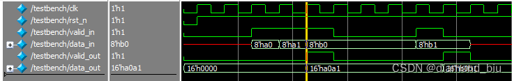
d_reg<=d;赋值语句需要写作阻塞赋值语句的形式,即先完成赋值操作,才能够输出out<=d_reg;。`timescale 1ns/1ns
module multi_sel(
input [7:0]d ,
input clk,
input rst,
output reg input_grant,
output reg [10:0]out
);
//*************code***********//
reg[1:0] current_state,next_state;
reg[7:0] d_reg;
always @ (posedge clk or negedge rst) begin
if(!rst) current_state<=2'b00;
else current_state<=next_state;
end
always @ (current_state) begin
next_state<=2'b00;
case(current_state)
2'b00:next_state<=2'b01;
2'b01:next_state<=2'b10;
2'b10:next_state<=2'b11;
2'b11:next_state<=2'b00;
endcase
end
always @ (posedge clk or negedge rst) begin
if(!rst) begin
input_grant<=0;
out<=0;
d_reg<=d;
end
else begin
case(current_state)
2'b00:begin input_grant<=1'b1;d_reg=d;out<=d_reg;end
2'b01:begin input_grant<=1'b0;out<= d_reg + {2'b0, d_reg, 1'b0};end
2'b10:begin input_grant<=1'b0;out<=d_reg + {2'b00, d_reg, 1'b0} + {1'b0 ,d_reg, 2'b00};end
2'b11:begin input_grant<=1'b0;out<={d_reg, 3'b000};end
endcase
end
end
//*************code***********//
endmodule
`timescale 1ns/1ns

module data_cal(
input clk,
input rst,
input [15:0]d,
input [1:0]sel,

output reg [4:0]out,
output reg validout
);
//*************code***********//
reg [15:0] reg_d;

always @ (posedge clk or rst or d) begin
    if(!rst) begin
        out<=5'b0;
		validout<=0;
    end
    else begin
        case(sel)
			2'b00:begin out<=5'b0; validout<=0; reg_d<=d ;end
			2'b01:begin out<=reg_d[3:0]+reg_d[7:4]; validout<=1; end
			2'b10:begin out<=reg_d[3:0]+reg_d[11:8]; validout<=1; end
			2'b11:begin out<=reg_d[3:0]+reg_d[15:12]; validout<=1; end
		endcase
    end
end
//*************code***********//
endmodule
always @ (posedge clk or negedge rst_n) 的写法是正确的,但有点疑惑是初始状态下就是低电平会不会触发,本题既然是正确的就说明初始低电平会触发。always @ (posedge clk or rst_n) 的写法是错误的,会在rst_n由0变为1时触发,但此时可能并非时钟上升沿,造成异常输出。always @ (posedge clk)的写法会使得初始状态下输出信号处于无效状态,额外在always块前加上initial c<=9'b0;这样可以通过测试用例,但是initial语句不可综合,最好不要使用。`timescale 1ns/1ns
module data_select(
input clk,
input rst_n,
input signed[7:0]a,
input signed[7:0]b,
input [1:0]select,
output reg signed [8:0]c
);
always @ (posedge clk or negedge rst_n) begin
if(!rst_n) begin
c<=9'b0;
end
else begin
case(select)
2'b00:begin c<=a; end
2'b01:begin c<=b; end
2'b10:begin c<=a+b; end
2'b11:begin c<=a-b; end
endcase
end
end
endmodule
genvar声明循环变量。begin-end之间插入赋值语句,begin后面必须声明循环实例的名称。generate-for常用来简化assign的赋值,assign data_out[i]=data_in[7-i];展开后的8条assign语句是并行赋值的。如,在6线-64线、8线-256线译码器中可以用来简化代码。`timescale 1ns/1ns
module gen_for_module(
input [7:0] data_in,
output [7:0] data_out
);
genvar i;
generate for(i=0;i<=7;i=i+1)
begin:label
assign data_out[i]=data_in[7-i];
end
endgenerate
endmodule
`timescale 1ns/1ns
module testbench();
	reg signed [7:0] a,b,c;
	reg clk,rst_n;
	wire [7:0]d;
main_mod dut(
	.clk(clk),
	.rst_n(rst_n),
	.a(a),
	.b(b),
	.c(c),
	.d(d)
);
always #5 clk = !clk;
initial begin
	clk=0;rst_n=0;
	#5 rst_n=1;
	#10 a=2;b=3;c=4;
	#10 a=4;b=2;c=1;
	#10 a=5;b=4;c=3;
end
endmodule
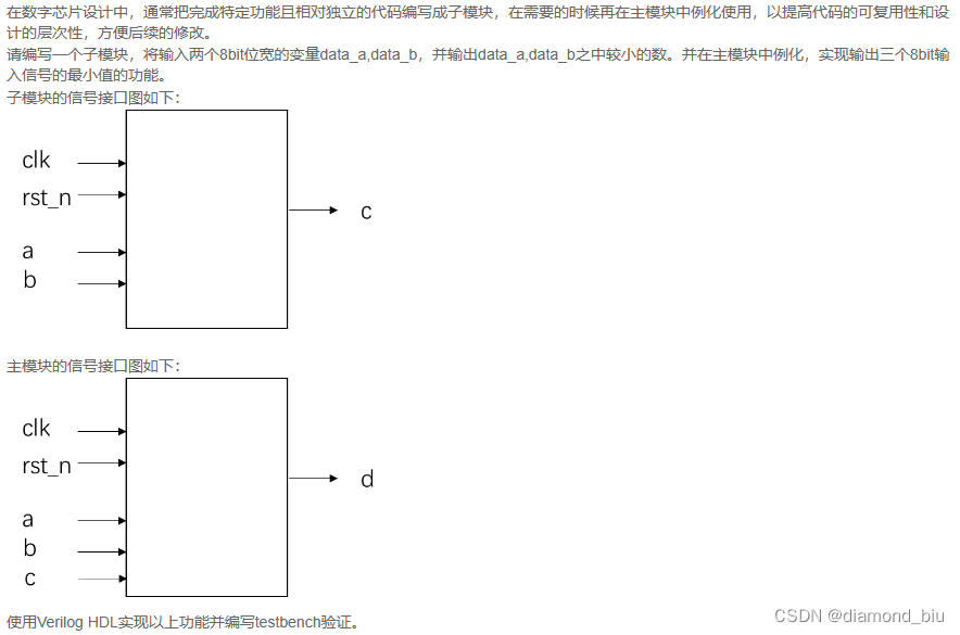
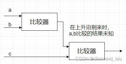
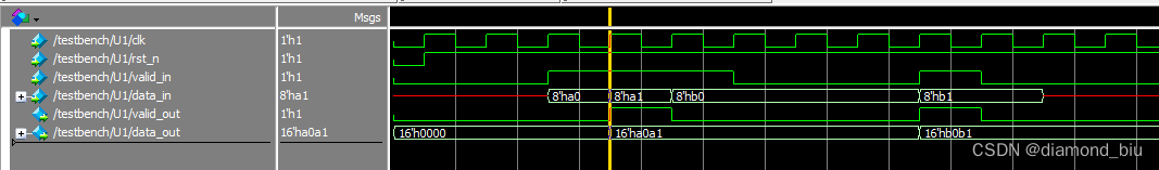
三个比较器的仿真波形如下。可以看到每一次比较的结果都在下一个时钟周期输出,分别为2,1,3。
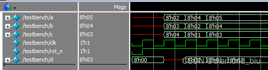
二个比较器的仿真波形如下,此时比较结果为1,2,3,这是因为上一轮a,b的最小值实际上是与当前周期的c进行比较的,因此对于第一组输入,a和b的比较结果是2,2和下一组输入的c=1进行了比较,所以输出的最小值是1;同样第二组输出,a和b的比较结果是2,2和下一组输入的c=3进行了比较,所以输出为2;第二组输出,a和b的比较结果是4,4和下一组输入的c=3进行了比较,所以输出为3。
c<=(a>b)?b:a;语句需要使用非阻塞赋值。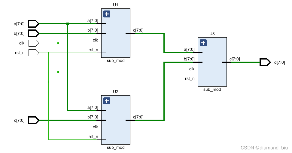
b <= a; :非阻塞赋值中赋值并不是马上执行的,也就是说"always"块内的下一条语句执行后,b并不等于a,而是保持原来的值。"always"块结束后,才进行赋值。b=a;:方式是马上执行的。也就是说执行下一条语句时,b已等于a。`timescale 1ns/1ns
module main_mod(
input clk,
input rst_n,
input [7:0]a,
input [7:0]b,
input [7:0]c,
output [7:0]d
);
wire [7:0] ab,ac;
sub_mod U1(.clk(clk),.rst_n(rst_n),.a(a),.b(b),.c(ab));
sub_mod U2(.clk(clk),.rst_n(rst_n),.a(a),.b(c),.c(ac));
sub_mod U3(.clk(clk),.rst_n(rst_n),.a(ab),.b(ac),.c(d));
endmodule
module sub_mod(clk,rst_n,a,b,c);
input clk,rst_n;
input[7:0] a,b;
output [7:0] c;
reg[7:0]c;
always@(posedge clk or negedge rst_n)begin
if(~rst_n)c<=8'b0;
else begin
c<=(a>b)?b:a;
end
end
endmodule
要点1:题目中说要用门级描述完成,对于1bit数的比较对应的门运算如下,A>B对应~A&B,A<B对应A&~B,A=B对应~(A^B)。
`timescale 1ns/1ns

module comparator_4(
	input		[3:0]       A   	,
	input	   [3:0]		B   	,

 	output	 wire		Y2    , //A>B
	output   wire        Y1    , //A=B
    output   wire        Y0      //A<B
);

assign Y2=(A[3]>B[3])|((A[3]==B[3])&(A[2]>B[2]))|((A[3]==B[3])&(A[2]==B[2])&(A[1]>B[1]))|((A[3]==B[3])&(A[2]==B[2])&(A[1]==B[1])&(A[0]>B[0]));
assign Y1=(A==B);
assign Y0=(A[3]<B[3])|((A[3]==B[3])&(A[2]<B[2]))|((A[3]==B[3])&(A[2]==B[2])&(A[1]<B[1]))|((A[3]==B[3])&(A[2]==B[2])&(A[1]==B[1])&(A[0]<B[0]));
endmodule
要点2:抽象描述可以写到直接比较A和B。
`timescale 1ns/1ns
module comparator_4(
	input		[3:0]       A   	,
	input	   [3:0]		B   	,
 	output	 wire		Y2    , //A>B
	output   wire        Y1    , //A=B
    output   wire        Y0      //A<B
);
assign Y2=(A>B)?1:0;
assign Y1=(A==B)?1:0;
assign Y0=(A<B)?1:0;
endmodule
1比特进位加法器的两种实现:
//实现1:逻辑代数
assign sum=a^b^cin;
assign cout=a&b|(cin&(a^b));或者assign cout=(a&b)|(a&cin)|(b&cin);
//实现2:抽象描述
assign {cout,sum}=a+b+cin;
assign cout=(a&b)|(a&cin)|(b&cin);很容易理解,即a,b,cin中任意两个或以上为1就进位。
assign cout=a&b|(cin&(a^b));可以理解为除了a,b为1的情况外,还有c为1同时 a和b中任意一个为1(a^b)。
多位数进位加法器
多位数进位加法器的实现有两种方式:串行进位加法器、超前进位加法器。
串行进位加法器就是将1比特加法器级联。
超前进位加法器是对串行全加器进行改良设计的并行加法器,以解决普通全加器串联互相进位产生的延迟。
一位全加器的进位的运算逻辑(前面的式子是(A^B)这里是(A|B),对结果没有影响,|包含了^):
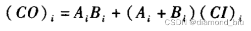
其中,令进位函数Gi = AiBi, 令进位传送函数Pi = Ai + Bi;
对于4比特超前进位加法器来说,进位输出如下:
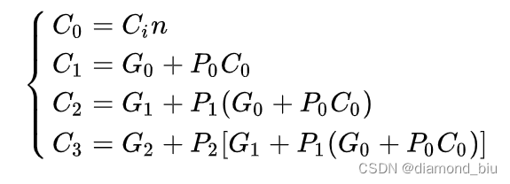
Si=Ai^Bi^(CI)i,对应的(CI)i=(CO)i-1,即Si=Ai^Bi^(CO)i-1。通过前面的推导已经得出了,可得:
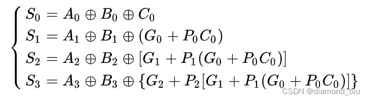
COi=(Ai&Bi)|(CIi&(Ai|Bi))。`timescale 1ns/1ns
module lca_4(
input [3:0] A_in ,
input [3:0] B_in ,
input C_1 ,
output wire CO ,
output wire [3:0] S
);
wire[3:0] g,p,c;
assign p=A_in|B_in;
assign g=A_in&B_in;
assign c[0]=g[0]|(p[0]&C_1);
assign c[1]=g[1]|(p[1]&(g[0]|(p[0]&C_1)));
assign c[2]=g[2]|(p[2]&(g[1]|(p[1]&(g[0]|(p[0]&C_1)))));
assign c[3]=g[3]|(p[3]&(g[2]|(p[2]&(g[1]|(p[1]&(g[0]|(p[0]&C_1)))))));
assign CO=c[3];
assign S=A_in^B_in^{c[2:0],C_1};
endmodule
测试代码:
`timescale 1ns/1ns
module testbench();
reg[3:0] A_in,B_in;
reg C_1;
wire CO;
wire[3:0] S;
reg[7:0] num;

lca_4 U1(.A_in(A_in),.B_in(B_in),.C_1(C_1),.CO(CO),.S(S));
initial begin
	C_1=0;
	num=0;
end
always #10 begin
	num=num+1;
	A_in<=num[3:0];
	B_in<=num[7:4];
end
endmodule
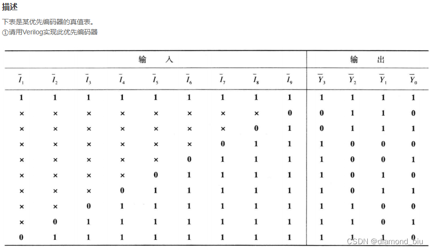
要点1:题目给的是I1-I9,注意顺序。
要点2:case、casez和casex三者都是可以综合的。case进行全等匹配,casez忽略?或z对应的位进行匹配,casex忽略x、?或z对应的位进行匹配。
`timescale 1ns/1ns
module encoder_0(
   input      [8:0]         I_n,
   output reg [3:0]         Y_n
);
always@(I_n)begin
	casez(I_n)
	9'b111111111:Y_n<=4'b1111;
	9'b0????????:Y_n<=4'b0110;
	9'b10???????:Y_n<=4'b0111;
	9'b110??????:Y_n<=4'b1000;
	9'b1110?????:Y_n<=4'b1001;
	9'b11110????:Y_n<=4'b1010;
	9'b111110???:Y_n<=4'b1011;
	9'b1111110??:Y_n<=4'b1100;
	9'b11111110?:Y_n<=4'b1101;
	9'b111111110:Y_n<=4'b1110;
	endcase
end
endmodule
要点3:《CPU设计实战》这本书中提到在CPU设计中必须遵守的硬性规定是代码中禁止出现casez、casex,因此可以采用如下写法,看Y9~Y0中出现的第一个0的位置。
`timescale 1ns/1ns
module encoder_0(
   input      [8:0]         I_n,
   output     [3:0]         Y_n
);
assign Y_n=(~I_n[8])?4'b0110:
		   (~I_n[7])?4'b0111:
		   (~I_n[6])?4'b1000:
		   (~I_n[5])?4'b1001:
		   (~I_n[4])?4'b1010:
		   (~I_n[3])?4'b1011:
		   (~I_n[2])?4'b1100:
		   (~I_n[1])?4'b1101:
		   (~I_n[0])?4'b1110:
					 4'b1111;
endmodule

题目描述的不是很清楚。
要点1:GS:按下为1,不按为0,需要注意的是最后assign GS=(S_n==10'b1111111111)?1'b0:1'b1;并不能只判断S_n[0]==1,因为其他按键(9~1)被按下时S_n[0]也为0;
要点2:最终的输出需要对译码结果取反assign L=~Y_n;
`timescale 1ns/1ns

module encoder_0(
   input      [8:0]         I_n   ,
   output     [3:0]         Y_n
);
assign Y_n=(~I_n[8])?4'b0110:
		   (~I_n[7])?4'b0111:
		   (~I_n[6])?4'b1000:
		   (~I_n[5])?4'b1001:
		   (~I_n[4])?4'b1010:
		   (~I_n[3])?4'b1011:
		   (~I_n[2])?4'b1100:
		   (~I_n[1])?4'b1101:
		   (~I_n[0])?4'b1110:
					 4'b1111;
endmodule

module key_encoder(
      input      [9:0]         S_n   ,
      output wire[3:0]         L     ,
      output wire              GS
);
    wire[3:0] Y_n;
    encoder_0 U1(.I_n(S_n[9:1]),.Y_n(Y_n));
    //GS:按下为1,不按为0
    assign GS=(S_n==10'b1111111111)?1'b0:1'b1;
    assign L=~Y_n;
endmodule
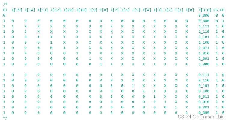
要点1:编码的结果为000时,可能有三种情况,(1)译码器没有使能,不工作,此时GS=0;EO=0;(2)译码器再工作,但无输入,GS=0;EO=1;;(3)译码器在工作,且有输入,输入为0000_0001,GS=1;EO=0;;
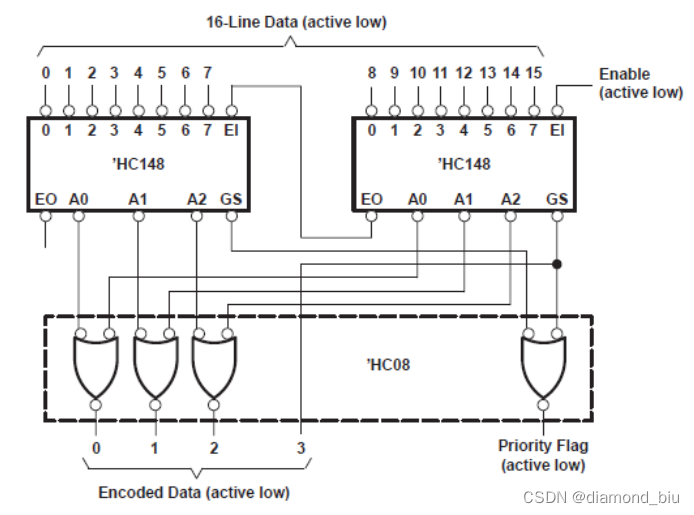
要点2:参考SNx4HC148 8-Line to 3-Line Priority Encoders理解如何使用两个8-3译码器得到一个16-4译码器。实际就是将两个8-3译码器的EO与EI连接,输出取或运算作为译码结果的低3位I[2:0],高位译码器的GS作为译码结果I[3](1表示高位译码器在译码15~8,0表示在译码0~7)。最终的GS为GS1|GS2。
真值表如下:
`timescale 1ns/1ns
module encoder_83(
   input      [7:0]       I   ,
   input                  EI  ,

   output wire [2:0]      Y   ,
   output wire            GS  ,
   output wire            EO
);
assign {Y,GS,EO}=(~EI)?5'b00000:
                  I[7]?5'b11110:
                  I[6]?5'b11010:
                  I[5]?5'b10110:
                  I[4]?5'b10010:
                  I[3]?5'b01110:
                  I[2]?5'b01010:
                  I[1]?5'b00110:
                  I[0]?5'b00010:
                       5'b00001;
endmodule

module encoder_164(
   input      [15:0]      A   ,
   input                  EI  ,

   output wire [3:0]      L   ,
   output wire            GS  ,
   output wire            EO
);
wire GS1,GS2,EO1;
wire[2:0] L1,L2;
encoder_83 U1(.I(A[15:8]),.EI(EI),.Y(L1[2:0]),.GS(GS1),.EO(EO1));
encoder_83 U2(.I(A[7:0]),.EI(EO1),.Y(L2[2:0]),.GS(GS2),.EO(EO));
assign L={GS1,L1|L2};
assign GS=GS1|GS2;
endmodule
要点1:最小项与最大项。
全减器真值表如下,可以看到对于A B Ci来说,从上到下一次为最小项m0~m7,因此D=m1+m2+m4+m7,Co=m1+m2+m3+m7。将A B Ci接入题中3-8译码器,译码器输出Yi对应的是mi取反。

`timescale 1ns/1ns

module decoder_38(
   input             E1_n   ,
   input             E2_n   ,
   input             E3     ,
   input             A0     ,
   input             A1     ,
   input             A2     ,

   output wire       Y0_n   ,
   output wire       Y1_n   ,
   output wire       Y2_n   ,
   output wire       Y3_n   ,
   output wire       Y4_n   ,
   output wire       Y5_n   ,
   output wire       Y6_n   ,
   output wire       Y7_n
);
wire E ;
assign E = E3 & ~E2_n & ~E1_n;
assign  Y0_n = ~(E & ~A2 & ~A1 & ~A0);
assign  Y1_n = ~(E & ~A2 & ~A1 &  A0);
assign  Y2_n = ~(E & ~A2 &  A1 & ~A0);
assign  Y3_n = ~(E & ~A2 &  A1 &  A0);
assign  Y4_n = ~(E &  A2 & ~A1 & ~A0);
assign  Y5_n = ~(E &  A2 & ~A1 &  A0);
assign  Y6_n = ~(E &  A2 &  A1 & ~A0);
assign  Y7_n = ~(E &  A2 &  A1 &  A0);
endmodule

module decoder1(
   input             A     ,
   input             B     ,
   input             Ci    ,

   output wire       D     ,
   output wire       Co
);
wire E3=1,E2_n=0,E1_n=0;
wire m0,m1,m2,m3,m4,m5,m6,m7;
decoder_38 U1(.E1_n(E1_n),.E2_n(E2_n),.E3(E3),
              .A0(Ci),.A1(B),.A2(A),
              .Y0_n(m0),.Y1_n(m1),.Y2_n(m2),.Y3_n(m3),.Y4_n(m4),.Y5_n(m5),.Y6_n(m6),.Y7_n(m7));
assign D=(~m1)|(~m2)|(~m4)|(~m7);
assign Co=(~m1)|(~m2)|(~m3)|(~m7);
endmodule
要点1:熟悉逻辑函数的两种表示形式,最小项和最大项。以本题为例,将逻辑表达式写为最小项形式,即L=m1+m3+m6+m7,又因为3-8译码器的输出恰好是最小项取反,以ABC=111为例,对应最小项m7=1,对应译码器输出为Y7=0,因此只需要将译码器输出取反即为对应的最小项的值。

要点2:题目中表达式的最大项表达式为L=M0+M3+M4+M5,其中M0=A+B+C。最大项表式可以由最小项表示推导出。
//module decoder_38省略,题目中直接给出了
module decoder0(
   input             A     ,
   input             B     ,
   input             C     ,
   output wire       L
);

wire E3=1,E2_n=0,E1_n=0;
wire m0,m1,m2,m3,m4,m5,m6,m7;
decoder_38 U1(.E1_n(E1_n),.E2_n(E2_n),.E3(E3),
              .A0(C),.A1(B),.A2(A),
              .Y0_n(m0),.Y1_n(m1),.Y2_n(m2),.Y3_n(m3),.Y4_n(m4),.Y5_n(m5),.Y6_n(m6),.Y7_n(m7));

assign  L=(~m1)|(~m3)|(~m6)|(~m7);

endmodule
要点1:牛客的题解写的很清楚了,化简后找对应项要动手推一下。
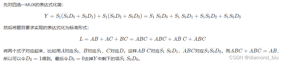
`timescale 1ns/1ns
module data_sel(
   input             S0     ,
   input             S1     ,
   input             D0     ,
   input             D1     ,
   input             D2     ,
   input             D3     ,

   output wire        Y
);

assign Y = ~S1 & (~S0&D0 | S0&D1) | S1&(~S0&D2 | S0&D3);
endmodule

module sel_exp(
   input             A     ,
   input             B     ,
   input             C     ,

   output wire       L
);
data_sel U1(.S0(A),.S1(B),.D0(0),.D1(~C),.D2(C),.D3(1),.Y(L));
endmodule
要点1:根据同步时序电路的设计方法,由状态转换表写出激励方程和输出函数即可。
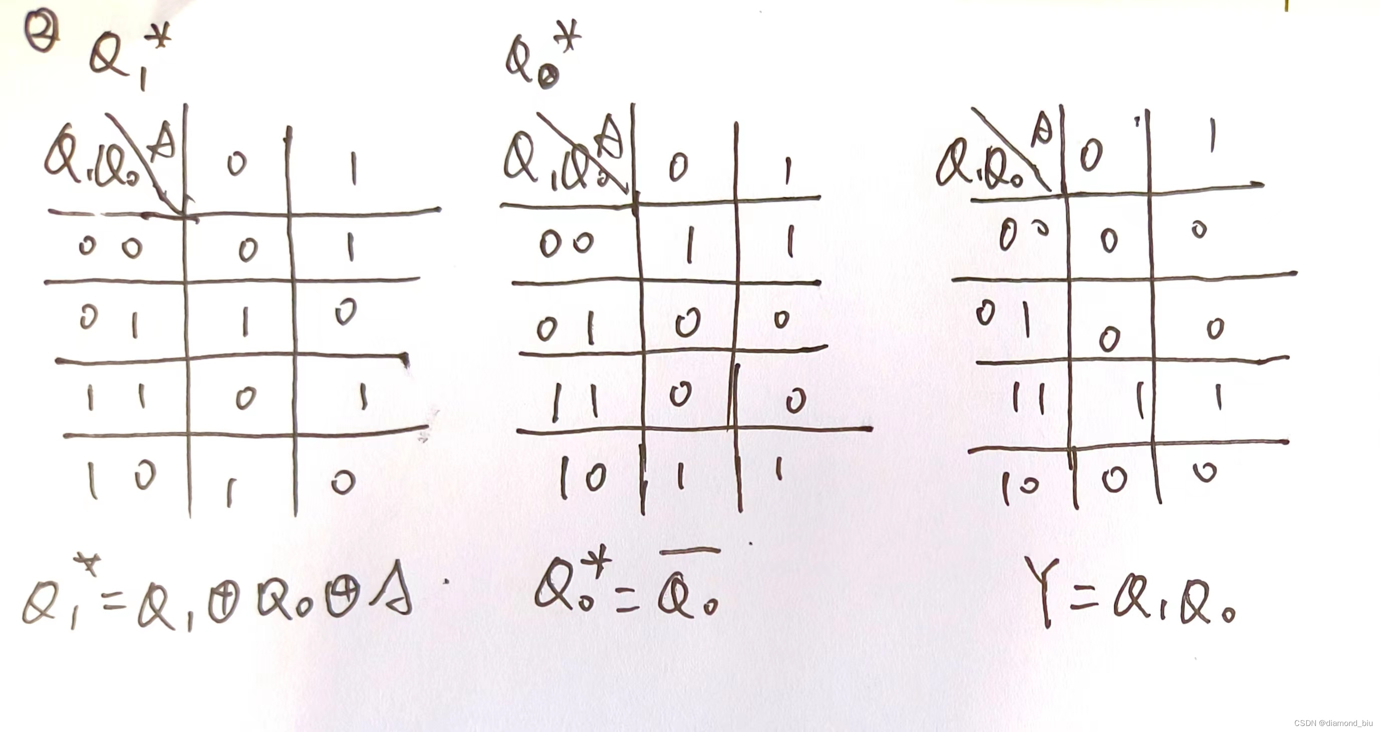
`timescale 1ns/1ns

module seq_circuit(
      input                A   ,
      input                clk ,
      input                rst_n,

      output   wire        Y
);
reg Q1,Q0;
always @ (posedge clk or negedge rst_n) begin
    if(!rst_n) begin
       Q1<=0;Q0<=0;
    end
    else begin
        Q1<=Q1^Q0^A;
		Q0<=~Q0;
    end
end
assign Y=Q1&Q0;
endmodule
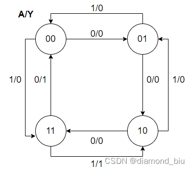
要点2:也可以采用有向状态机的写法。状态转移图如下:
经典三段式
`timescale 1ns/1ns

module seq_circuit(
      input                A   ,
      input                clk ,
      input                rst_n,

      output   reg        Y
);

reg[1:0] current_state,next_state;
always @ (posedge clk or negedge rst_n) begin
    if(!rst_n) current_state<=2'b00;
    else current_state<=next_state;
end
always @ (current_state or A) begin
    next_state<=2'b00;
	case(current_state)
	2'b00:begin
		if(A)next_state<=2'b11;
		else next_state<=2'b01;
	end
	2'b01:begin
		if(A)next_state<=2'b00;
		else next_state<=2'b10;
	end
	2'b10:begin
		if(A)next_state<=2'b01;
		else next_state<=2'b11;
	end
	2'b11:begin
		if(A)next_state<=2'b10;
		else next_state<=2'b00;
	end
	endcase
end
always @ (*) begin
    case(current_state)
	2'b00:begin
		if(A)Y<=0;
		else Y<=0;
	end
	2'b01:begin
		if(A)Y<=0;
		else Y<=0;
	end
	2'b10:begin
		if(A)Y<=0;
		else Y<=0;
	end
	2'b11:begin
		if(A)Y<=1;
		else Y<=1;
	end
	endcase
end

endmodule
与VL21类似。
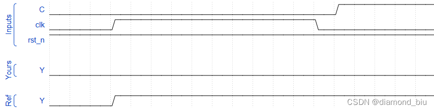
要点1:同步时序电路设计流程,需要注意的是Y需要写成组合逻辑。
`timescale 1ns/1ns

module seq_circuit(
   input                C   ,
   input                clk ,
   input                rst_n,

   output   wire        Y
);
reg Q1,Q0;
always @ (posedge clk or negedge rst_n) begin
    if(!rst_n) begin
		Q0<=0;Q1<=0;
    end
    else begin
        Q1<=(Q0&(~C))|(Q1&C);
		Q0<=(Q0&(~C))|((~Q1)&C);
    end
end
assign Y=(Q1&Q0)|(Q1&C);
endmodule
要点2:状态机经典三段式。
`timescale 1ns/1ns

module seq_circuit(
   input                C   ,
   input                clk ,
   input                rst_n,

   output   reg        Y
);
reg[1:0] current_state,next_state;
always @ (posedge clk or negedge rst_n) begin
    if(!rst_n) current_state<=2'b00;
    else current_state<=next_state;
end
always @ (current_state or C) begin
    next_state<=2'b00;
	case(current_state)
	2'b00:begin
		if(C)next_state<=2'b01;
		else next_state<=2'b00;
	end
	2'b01:begin
		if(C)next_state<=2'b01;
		else next_state<=2'b11;
	end
	2'b10:begin
		if(C)next_state<=2'b10;
		else next_state<=2'b00;
	end
	2'b11:begin
		if(C)next_state<=2'b10;
		else next_state<=2'b11;
	end
	endcase
end
always @ (*) begin
    case(current_state)
	2'b00:begin
		if(C)Y<=0;
		else Y<=0;
	end
	2'b01:begin
		if(C)Y<=0;
		else Y<=0;
	end
	2'b10:begin
		if(C)Y<=1;
		else Y<=0;
	end
	2'b11:begin
		if(C)Y<=1;
		else Y<=1;
	end
	endcase
end
endmodule
要点1:根据题目给出的反例可以看到,在非时钟上升沿,输入的addr改变,输出的data也会改变,因此data=rom_array[addr];这一赋值应该是组合逻辑而非时序逻辑。反例如下:
//这种写法不正确
/*
`timescale 1ns/1ns
module rom(
	input clk,
	input rst_n,
	input [7:0]addr,

	output reg[3:0]data
);
reg[0:3] rom_array [7:0];
always @ (posedge clk or negedge rst_n) begin
    if(!rst_n) begin
		rom_array[0]<=4'd0;
		rom_array[1]<=4'd2;
		rom_array[2]<=4'd4;
		rom_array[3]<=4'd6;
		rom_array[4]<=4'd8;
		rom_array[5]<=4'd10;
		rom_array[6]<=4'd12;
		rom_array[7]<=4'd14;
        data<=0;
    end
    else begin
        data<=rom_array[addr];
    end
end
endmodule
*/
`timescale 1ns/1ns
module rom(
	input clk,
	input rst_n,
	input [7:0]addr,

	output [3:0]data
);

reg[0:3] rom_array [7:0];

always @ (posedge clk or negedge rst_n) begin
    if(!rst_n) begin
		rom_array[0]<=4'd0;
		rom_array[1]<=4'd2;
		rom_array[2]<=4'd4;
		rom_array[3]<=4'd6;
		rom_array[4]<=4'd8;
		rom_array[5]<=4'd10;
		rom_array[6]<=4'd12;
		rom_array[7]<=4'd14;
    end
    else ;
end
assign data=rom_array[addr];
endmodule
要点1:参考Verilog设计(四):边沿检测。将原始波形a分别延迟1拍、2拍得到a[0]和a[1],上升沿检测即a[0]&(~a[1]),下降沿检测即(~a[0])&a[1]。
图中边沿检测多延迟了一拍。
本题用a0存储a的上一个状态,01((~a0)&a)即为上升沿,10即为下降沿(a0(~a)),其余情况既不是上升沿也不是下降沿。
`timescale 1ns/1ns
module edge_detect(
	input clk,
	input rst_n,
	input a,

	output reg rise,
	output reg down
);
reg a0;
always @ (posedge clk or negedge rst_n) begin
    if(!rst_n) begin
        rise<=0;down<=0;
    end
    else begin
    	a0<=a;
		if(a&(~a0))rise<=1;
		else if((~a)&a0)down<=1;
		else begin
			rise<=0;down<=0;
		end
    end
end

endmodule
要点2:用状态机写,共有3个状态。在{reg_a,a}改变时发生状态转移。(这是sh的写法
`timescale 1ns/1ns
module edge_detect(
	input clk,
	input rst_n,
	input a,

	output reg rise,
	output reg down
);

reg [1:0]current_state;
reg [1:0]next_state;
reg reg_a;

always @(posedge clk or negedge rst_n) begin
	if (!rst_n) current_state <= 0;
	else current_state <= next_state;
end

always @(*) begin
	case (current_state)
		2'b00:begin
			rise = 0;
			down = 0;
		end
		2'b01:begin
			rise = 1;
			down = 0;
		end
		2'b10:begin
			rise = 0;
			down = 1;
		end
		2'b11:begin
			rise = 0;
			down = 0;
		end
	endcase
end

always @(posedge clk or negedge rst_n)begin
	if (!rst_n) reg_a <= 0;
	else reg_a <= a;
end

always @(a or reg_a) begin
	case ({reg_a,a})
		2'b00:next_state = 2'b00;
		2'b01:next_state = 2'b01;
		2'b10:next_state = 2'b10;
		2'b11:next_state = 2'b00;
	endcase
end

endmodule
要点3:还是状态机(我的写法,找了两天bug的结果,心累…
current_state和next_state的初始状态要设置为11,但是由于这是查看错误样例后才知道的,因此需要添加的idle作为初始无效状态,当检测到有效信号后再进入对应状态,0则进入00状态,1则进入11状态。if(a==1)...;else...;本意是a为1和0时分别跳转到下一个状态,但由于所给测试向量存在无效状态,因此条件判断改为了if(a==1)...;else if(a==0)...;else next_state=idle;这样就可以在出现无效状态时不产生异常的状态跳转。case(next_state),如果写成组合逻辑为case(current_state),两种写法在下示代码都有显示。`timescale 1ns/1ns
module edge_detect(
input clk,
input rst_n,
input a,
output reg rise,
output reg down
);
parameter idle=3'b111;
reg[2:0] current_state,next_state;
always @ (posedge clk or negedge rst_n) begin
if(!rst_n)current_state<=idle;
else current_state<=next_state;
end
always @ (current_state or a) begin
next_state=idle;
case(current_state)
3'b000:begin
if(a==1)next_state=3'b001;
else if(a==0)next_state=3'b000;
else next_state=idle;
end
3'b001:begin
if(a==1)next_state=3'b011;
else if(a==0) next_state=3'b010;
else next_state=idle;
end
3'b010:begin
if(a==1)next_state=32'b001;
else if(a==0)next_state=3'b000;
else next_state=idle;
end
3'b011:begin
if(a==1)next_state=3'b011;
else if(a==0)next_state=3'b010;
else next_state=idle;
end
idle:begin
if(a==1)next_state=3'b011;
else if(a==0)next_state=3'b000;
else next_state=idle;
end
default:next_state=idle;
endcase
end
always@(*)begin
case(current_state)
3'b000:begin rise=0;down=0;end
3'b001:begin rise=1;down=0;end
3'b010:begin rise=0;down=1; end
3'b011:begin rise=0;down=0; end
3'b111:begin rise=0;down=0;end
default:begin rise=0;down=0; end
endcase
end
/*
always @(posedge clk or negedge rst_n)begin
if(~rst_n)begin
rise<=0;down<=0;
end
else begin
case(next_state)
3'b000:begin rise<=0;down<=0;end
3'b001:begin rise<=1;down<=0;end
3'b010:begin rise<=0;down<=1; end
3'b011:begin rise<=0;down<=0; end
3'b111:begin rise<=0;down<=0;end
default:begin rise<=0;down<=0; end
endcase
end
end
*/
endmodule
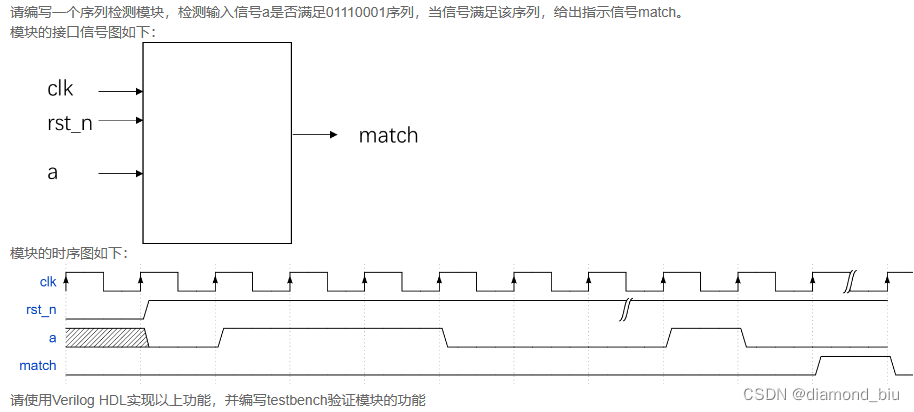
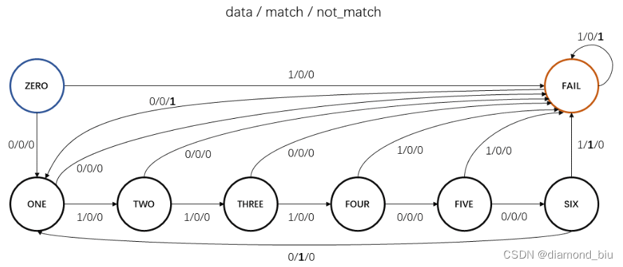
要点1:使用优先状态机,经典三段式。
s0:初始状态,没有匹配到任何序列;
s1:匹配到序列'0';
…
s8:匹配到序列'01110001';
需要的注意的状态跳转遇到不匹配时并不是直接跳转回s0,应该跳转回最长匹配子序列对应的状态。
`timescale 1ns/1ns
module sequence_detect(
	input clk,
	input rst_n,
	input a,
	output reg match
	);
	parameter s0=4'd0,s1=4'd1,s2=4'd2,s3=4'd3,
			  s4=4'd4,s5=4'd5,s6=4'd6,s7=4'd7,s8=4'd8;
	reg[3:0] current_state,next_state;
	always @ (posedge clk or negedge rst_n) begin
		if(~rst_n) current_state<=s0;
		else current_state<=next_state;
	end

	always @ (a,current_state)begin
		next_state=s0;
		case(current_state)
		s0:next_state=a?s0:s1;
		s1:next_state=a?s2:s1;
		s2:next_state=a?s3:s1;
		s3:next_state=a?s4:s1;
		s4:next_state=a?s0:s5;
		s5:next_state=a?s2:s6;
		s6:next_state=a?s2:s7;
		s7:next_state=a?s8:s1;
		s8:next_state=a?s3:s1;
		default:next_state=s0;
		endcase
	end

	always @ (posedge clk or negedge rst_n) begin
		if(!rst_n) match<=0;
		else begin
			case(current_state)
			s8:match<=1;
			default:match<=0;
			endcase
		end
	end

endmodule
要点2:8bit线性移位寄存器,使用8位寄存器寄存历史序列,并与目标序列比较。
`timescale 1ns/1ns
module sequence_detect(
	input clk,
	input rst_n,
	input a,
	output reg match
	);
	reg[7:0] q;
	always @ (posedge clk or negedge rst_n) begin
		if(!rst_n) begin
			q<=8'b0;
		end
		else begin
			q<={q[6:0],a};
		end
	end

	always @ (posedge clk or negedge rst_n) begin
		if(!rst_n) begin
			match<=0;
		end
		else begin
			if(q==8'b01110001)match<=1;
			else match<=0;
		end
	end
endmodule
? :替代if-else,前者会让代码逻辑看起来更清晰。`timescale 1ns/1ns
module sequence_detect(
input clk,
input rst_n,
input data,
output reg match,
output reg not_match
);
reg[2:0] current_state,next_state;
reg[2:0] count;
always @ (posedge clk or negedge rst_n) begin
if(!rst_n) count<=0;
else count=((count==3'd6)?1:count+1);
end
always @ (posedge clk or negedge rst_n) begin
if(!rst_n) current_state<=3'b000;
else current_state<=next_state;
end
always@(*)begin
if(!rst_n)next_state=3'b000;
case(current_state)
3'b000:next_state=data?3'b111:3'b001;
3'b001:next_state=data?3'b010:3'b111;
3'b010:next_state=data?3'b011:3'b111;
3'b011:next_state=data?3'b100:3'b111;
3'b100:next_state=data?3'b111:3'b101;
3'b101:next_state=data?3'b111:3'b110;
3'b110:next_state=data?3'b111:3'b001;
3'b111:next_state=(count==6?3'b001:3'b111);
default:next_state=3'b000;
endcase
end
always @ (posedge clk or negedge rst_n) begin
if(!rst_n) begin
match<=0;
not_match<=0;
end
else begin
match<=(count==3'd6&&next_state==3'b110);
not_match<=(count==3'd6&&next_state==3'b111);
end
end
endmodule
要点1:虽然题目需要用状态机,但是第一反应肯定不是状态机,用移位寄存器更简单。
要点2:没有忘记用三目运算符,以及把temp赋值逻辑和match输出逻辑分开写了,有进步。
`timescale 1ns/1ns
module sequence_detect(
	input clk,
	input rst_n,
	input data,
	input data_valid,
	output reg match
	);

reg[3:0] temp;
always @ (posedge clk or negedge rst_n) begin
    if(!rst_n) temp<=4'b0000;
    else temp<=(data_valid)?{temp[2:0],data}:temp;
end
always @ (posedge clk or negedge rst_n) begin
    if(!rst_n) match<=0;
	else match<=temp[2:0]==3'b011&&data==1'b0&&data_valid;
end
endmodule
要点3:状态转移图如下,看题意应该是重叠序列检测。
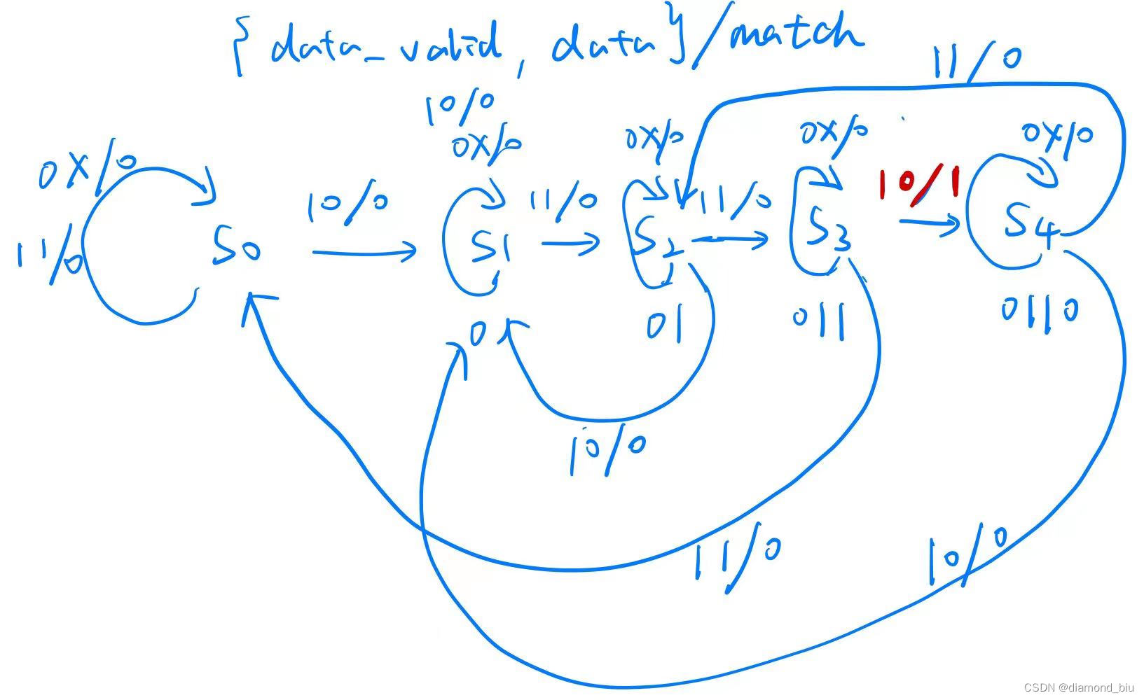
`timescale 1ns/1ns
module sequence_detect(
    input clk,
    input rst_n,
    input data,
    input data_valid,
    output reg match
    );
    parameter   s0 = 4'd0,
                s1 = 4'd1,
                s2 = 4'd2,
                s3 = 4'd3,
                s4 = 4'd4;
	reg[3:0] current_state,next_state;
	always @ (posedge clk or negedge rst_n) begin
		if(!rst_n) current_state<=s0;
		else current_state<=next_state;
	end
	always@(*)begin
		next_state=s0;
		case(current_state)
		s0:next_state=data_valid?(data?s0:s1):s0;
		s1:next_state=data_valid?(data?s2:s1):s1;
		s2:next_state=data_valid?(data?s3:s1):s2;
		s3:next_state=data_valid?(data?s0:s4):s3;
		s4:next_state=data_valid?(data?s2:s1):s4;
		endcase
	end
	always @ (posedge clk or negedge rst_n) begin
		if(!rst_n) match<=0;
		else match<=(next_state==s4)&(current_state==s3);
	end
endmodule
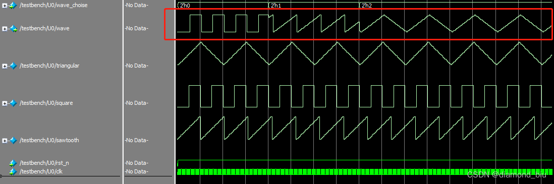
x !!!下面这个写法和题意不符!!!
`timescale 1ns/1ns
//wave的最大值是20
//三角波的周期是40
module triangular_wave(
	input clk,
	input rst_n,
	output reg [4:0]wave
	);
	reg current_state,next_state;
	always @ (posedge clk or negedge rst_n) begin
		if(!rst_n) current_state<=1'b1;
		else current_state<=next_state;
	end
	always @ (*) begin
		next_state<=1'b1;
		case(current_state)
		1'b0:next_state<=(wave==5'd20)?1'b1:1'b0;
		1'b1:next_state<=(wave==5'd0)?1'b0:1'b1;
		default:next_state<=0;
		endcase
	end
	always @ (posedge clk) begin
		case(next_state)
		1'b0:wave<=wave+1;
		1'b1:wave<=wave-1;
		default:wave<=0;
		endcase
	end

endmodule

//锯齿波的周期是21
module sawtooth_wave(
	input clk,
	input rst_n,
	output reg [4:0]wave
	);
	always @ (posedge clk or negedge rst_n) begin
		if(!rst_n)wave<=0;
		else wave<=(wave==5'd20)?0:wave+1;
	end
endmodule

//方波的周期是20,占空比百分之50
module square_wave(
	input clk,
	input rst_n,
	output reg [4:0]wave
	);
	reg[5:0]count;
	always @ (posedge clk or negedge rst_n) begin
		if(!rst_n )count<=0;
		else count<=(count==5'd19)?0:count+1;
	end

	always @ (posedge clk) begin
		wave<=(count<=9)?5'd0:5'd20;
	end
endmodule

module signal_generator(
	input clk,
	input rst_n,
	input [1:0] wave_choise,
	output reg [4:0]wave
	);
	wire[4:0] square,sawtooth,triangular;
	square_wave U1(.clk(clk),.rst_n(rst_n),.wave(square));
	sawtooth_wave U2(.clk(clk),.rst_n(rst_n),.wave(sawtooth));
	triangular_wave U3(.clk(clk),.rst_n(rst_n),.wave(triangular));

	always @ (posedge clk or negedge rst_n) begin
		if(!rst_n) begin
			wave<=0;
		end
		else begin
			case(wave_choise)
			2'b00:wave<=square;
			2'b01:wave<=sawtooth;
			2'b10:wave<=triangular;
			endcase
		end
	end
endmodule
2'b00:begin wave<=(count==9)? 5'd20 :(count==19 ? 5'd0 : wave); end,这个最开始写的是2'b00:begin wave<=(count<=9)?5'd0:5'd20; end,提交波形显示晚了一个时钟周期,但其实感觉这样写才比较合理,下面的写法会导致方波最开始宽度只有9,后面才正常为10。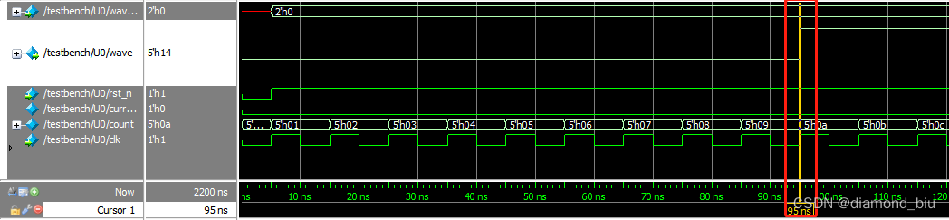
`timescale 1ns/1ns
module signal_generator(
input clk,
input rst_n,
input [1:0] wave_choise,
output reg [4:0]wave
);
reg[4:0]count;
//count其余模式置0,方波模式开始计数,周期为20
always @ (posedge clk or negedge rst_n) begin
if(!rst_n )count<=0;
else count<=(wave_choise==2'd0)?(count==5'd19 ? 5'd0 : count+1): 5'd0;
end
//三角波的周期是40,初始状态为,current_state=1为上升,0为下降
reg current_state;
always @ (posedge clk or negedge rst_n) begin
if(!rst_n) current_state<=1'b0;
//如果是三角波,使用current_state表示上升下降,如果只判断(wave==1)波形会012101210。
else current_state<=(wave_choise==2'd2)? (wave==1&¤t_state==0 ? 1 : (wave==19&¤t_state==1)? 0 : current_state) : 1'b0;
end
always @ (posedge clk or negedge rst_n) begin
if(!rst_n) begin
wave<=0;
end
else begin
case(wave_choise)
2'b00:begin wave<=(count==9)? 5'd20 :(count==19 ? 5'd0 : wave); end
2'b01:begin wave<=(wave==5'd20)?0:wave+1; end
2'b10:begin wave<=current_state?wave+1:wave-1; end
default wave<=0;
endcase
end
end
endmodule
将data_a单比特输入,每6位拼接成data_b输出。
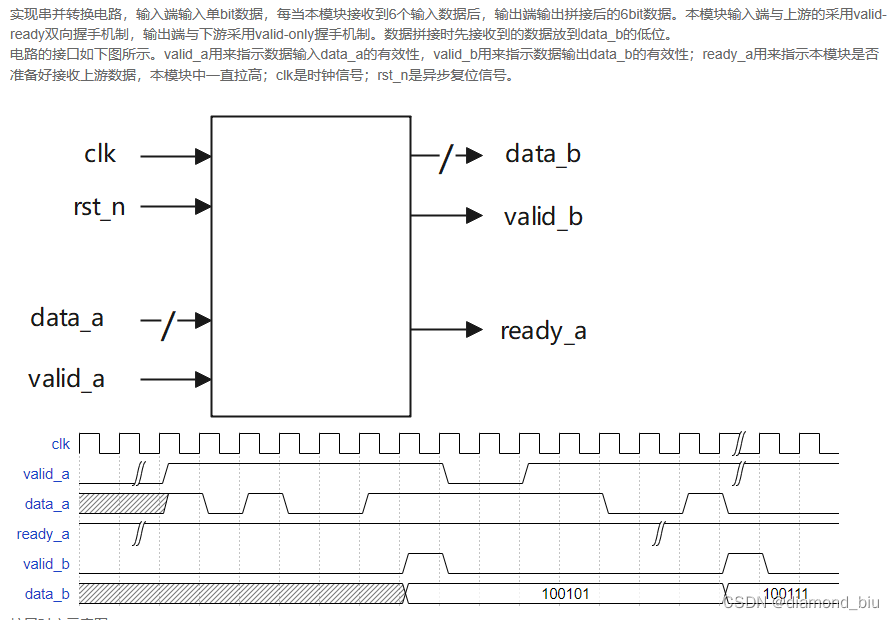
ready_a恒为高逻辑,count计数逻辑,reg_b移位寄存逻辑以及最后的data_b输出逻辑,分别写在四个过程块里面。data_b只在接到连续六个有效输入后才变化,因此需要reg_b寄存历史输入,data_b只在valid_b有效时才从reg_b获取。data_b<=(count==5&&valid_a&&ready_a)?reg_b:data_b;仿真波形可以看出问题所在,data_b输出的是6’h25,实际输出的是6’h0a,应该需要对data_b进行和reg_b相同的赋值操作,即data_b<=(count==5&&valid_a&&ready_a)?{data_a,reg_b[5:1]}:data_b;。data_b获取的是上一个周期reg_b的值。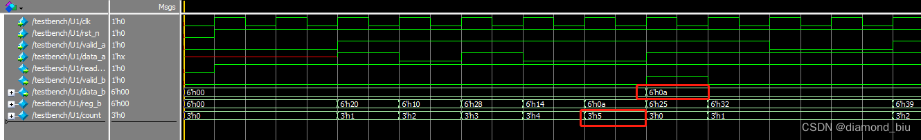
`timescale 1ns/1ns

module s_to_p(
	input 				clk 		,
	input 				rst_n		,
	input				valid_a		,
	input	 			data_a		,

 	output	reg 		ready_a		,
 	output	reg			valid_b		,
	output  reg [5:0] 	data_b
);
reg[5:0] reg_b;
reg[2:0] count;
always @ (posedge clk or negedge rst_n) begin
    if(!rst_n) ready_a<=1'b0;
    else ready_a=1'b1;
end
always @ (posedge clk or negedge rst_n) begin
    if(!rst_n) count<=0;
    else count<=(valid_a&ready_a)?(count==3'd5 ? 3'd0:count+1):count;
end
always @ (posedge clk or negedge rst_n) begin
    if(!rst_n) reg_b<=0;
    else reg_b<=(valid_a&ready_a)?{data_a,reg_b[5:1]}:reg_b;
end

always @ (posedge clk or negedge rst_n) begin
    if(!rst_n)begin
		valid_b<=0;
		data_b<=0;
	end
    else begin
		valid_b<=(count==5&&valid_a&&ready_a)?1:0;
		data_b<=(count==5&&valid_a&&ready_a)?{data_a,reg_b[5:1]}:data_b;
	end
end
endmodule
ready_a为1告诉上游可以正常接受数据,即上游可以发数据。如果下游ready_b拉高,表示下游可以接收模块输出数据,那么此时ready_a应拉高;同时,如果valid_b为低,表示4个数据还没收完,所以也拉高继续接收。valid_b为高告诉下游本模块在发数据了。当和上游正常通讯时(即valid_a&ready_a),数据正常接收,但注意计数了4个就得加起来输出一次,所以data_cnt == 2’d3时拉高valid_b;而等待下游接收,即当ready_a也拉高表示接收完成,则拉低valid_b,保证只有在四个数之和的时候才拉高。data_out: 当和上游正常通讯时(即valid_a&ready_a均为高),数据正常接收,数据累加,当计数器data_cnt == 2’d0表示需要从头再加,清零,但注意需要等到ready_b拉高,表示下游接收完成才能清空重新累加。`timescale 1ns/1ns
module valid_ready(
input clk ,
input rst_n ,
input [7:0] data_in ,
input valid_a ,
input ready_b ,
output ready_a ,
output reg valid_b ,
output reg [9:0] data_out
);
assign ready_a=~valid_b|ready_b;
reg[1:0] count;
always @ (posedge clk or negedge rst_n) begin
if(!rst_n) count<=0;
else count<=valid_a&&ready_a ? count+1 : count;
end
always @ (posedge clk or negedge rst_n) begin
if(!rst_n) valid_b<=0;
else valid_b<=(count==3&&valid_a&&ready_a) ? 1 : (valid_b&&ready_b) ? 0 : valid_b;
end
always @ (posedge clk or negedge rst_n) begin
if(!rst_n) data_out<=0;
else data_out<=(valid_a&&ready_a&&count==0&&ready_b) ? data_in : (valid_a&&ready_a) ? data_in+data_out : data_out;
end
endmodule
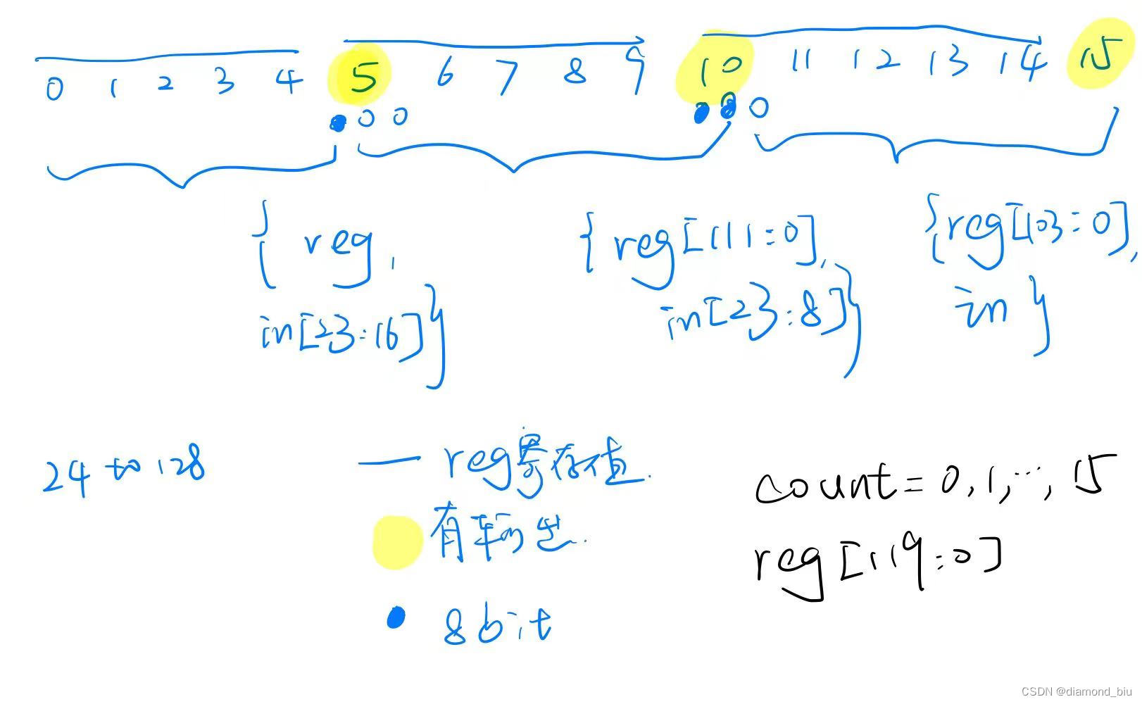
`timescale 1ns/1ns
module width_24to128(
	input 				clk 		,
	input 				rst_n		,
	input				valid_in	,
	input	[23:0]		data_in		,

 	output	reg			valid_out	,
	output  reg [127:0]	data_out
	);
	reg[119:0] data_reg;
	reg[3:0] count;
	always @ (posedge clk or negedge rst_n) begin
		if(!rst_n) count<=0;
		else count<=valid_in?((count==15) ? 0 : count+1 ):count;
	end

	always @ (posedge clk or negedge rst_n) begin
		if(!rst_n) data_reg<=0;
		else data_reg<=valid_in?{data_reg[103:0],data_in}:data_reg;
	end

	always @ (posedge clk or negedge rst_n) begin
		if(!rst_n) begin
			valid_out<=0;data_out<=0;
		end
		else begin
		case({count,valid_in})
			5'b01011:begin valid_out<=1; data_out<={data_reg,data_in[23:16]};end
			5'b10101:begin valid_out<=1; data_out<={data_reg[111:0],data_in[23:8]};end
			5'b11111:begin valid_out<=1; data_out<={data_reg[103:0],data_in};end
			default:begin valid_out<=0;data_out<=data_out;end
		endcase

		end
	end
endmodule
要点1:使用count记录状态,同时使用data_reg寄存历史8位数据。8to12一共有三个状态,(1)输入8位,无输出;(2)再输入8位,输出{data_reg,data_in[7:4]};(3)再输入8位,输出{data_reg[3:0],data_in};这三个状态循环出现,再valid_in==1时变化。
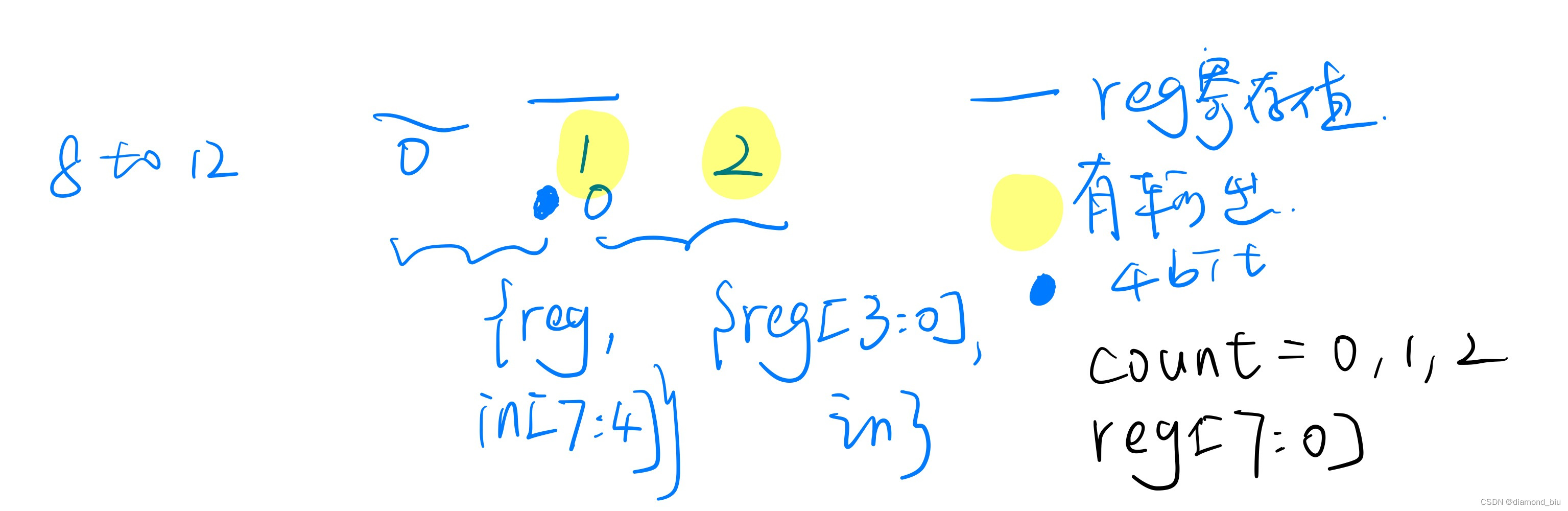
要点2:一共分为三个过程块来写,count计数块、data_reg历史输入寄存块、输出块。
要点3:还犯了一个很蠢的错误,case部分3’b101直接写成了101导致状态一直达不到。
`timescale 1ns/1ns

module width_8to12(
	input 				   clk 		,
	input 			      rst_n		,
	input				      valid_in	,
	input	[7:0]			   data_in	,

 	output  reg			   valid_out,
	output  reg [11:0]   data_out
	);
	reg[7:0] data_reg;
	reg [1:0]count;
	always @ (posedge clk or negedge rst_n) begin
		if(!rst_n) count<=0;
		else count<=valid_in?((count==2) ? 0 : count+1 ):count;
	end

	always @ (posedge clk or negedge rst_n) begin
		if(!rst_n) data_reg<=0;
		else data_reg<=valid_in?data_in:data_reg;
	end

	always @ (posedge clk or negedge rst_n) begin
		if(!rst_n) begin
			valid_out<=0;data_out<=0;
		end
		else begin
		case({count,valid_in})
			3'b011:begin valid_out<=1; data_out<={data_reg,data_in[7:4]};end
			3'b101:begin valid_out<=1; data_out<={data_reg[3:0],data_in};end
			default:begin valid_out<=0;data_out<=data_out;end
		endcase
		end
	end
endmodule
always @(posedge clk) data_in=data_in+1;。
module DFF(
	input clk ,
	input data_in,
	output reg data_reg
	);
	always @ (posedge clk) begin
		data_reg<=data_in;
	end
endmodule
`timescale 1ns/1ns
module testbench();
	reg clk;
	reg data_in;
	wire data_reg;

	initial beginclk=1;data_in=0;end
	always#5 clk=~clk;
	test U1(clk,data_in,data_reg);
	always @(posedge clk) data_in=data_in+1;
endmodule
第一种:
valid_out<=(count==2);
data_out<=(count==2)?reg_out:data_out;
第二种:
valid_out<=(count==1)&&valid_in;
data_out<=(count==1)&&valid_in?{reg_out[7:0],data_in}:data_out;
`timescale 1ns/1ns
module width_8to16(
	input 				   clk 		,
	input 				   rst_n		,
	input				      valid_in	,
	input	   [7:0]		   data_in	,

 	output	reg			valid_out,
	output   reg [15:0]	data_out
	);
	reg [15:0] reg_out;
	reg [0:1]count;

	always @ (posedge clk or negedge rst_n) begin
		if(!rst_n) count<=0;
		else count<=(count==2)?1:(valid_in ? count+1:count);
	end

	always @ (posedge clk or negedge rst_n) begin
		if(!rst_n) reg_out<=0;
		else reg_out<=valid_in?{reg_out[7:0],data_in}:reg_out;
	end

	always @ (posedge clk or negedge rst_n) begin
		if(!rst_n) begin
			valid_out<=0;data_out<=0;
		end
		else begin
			valid_out<=(count==1)&&valid_in;
			data_out<=(count==1)&&valid_in?{reg_out[7:0],data_in}:data_out;
		end
	end
endmodule
`timescale 1ns/1ns
module width_8to16(
	input 				   clk 		,
	input 				   rst_n		,
	input				      valid_in	,
	input	   [7:0]		   data_in	,

 	output	reg			valid_out,
	output   reg [15:0]	data_out
	);
	reg [7:0] data_reg;
	reg count;
	always @ (posedge clk or negedge rst_n) begin
		if(!rst_n) count<=0;
		else count<=valid_in?((count==1) ? 0 : count+1 ):count;
	end
	always @ (posedge clk or negedge rst_n) begin
		if(!rst_n) data_reg<=0;
		else data_reg<=valid_in?data_in:data_reg;
	end
	always @ (posedge clk or negedge rst_n) begin
		if(!rst_n) begin
			valid_out<=0;data_out<=0;
		end
		else begin
		case({count,valid_in})
			2'b11:begin valid_out<=1; data_out<={data_reg,data_in};end
			default:begin valid_out<=0;data_out<=data_out;end
		endcase
		end
	end
endmodule
flag<=current_state==3'b100&&data==1;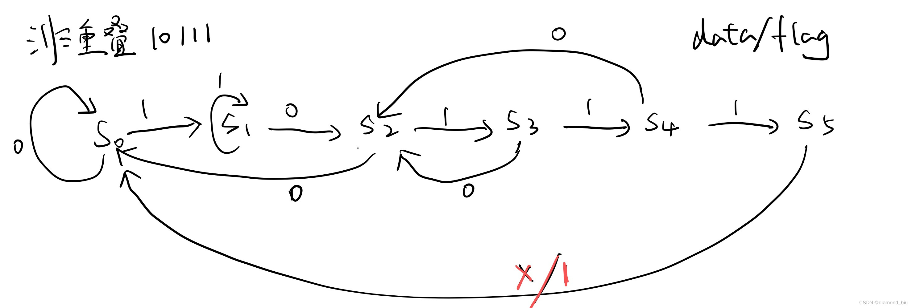
flag<=current_state==3'b100;,和VL35的输出周期竟然还不一样,,,牛客好奇怪。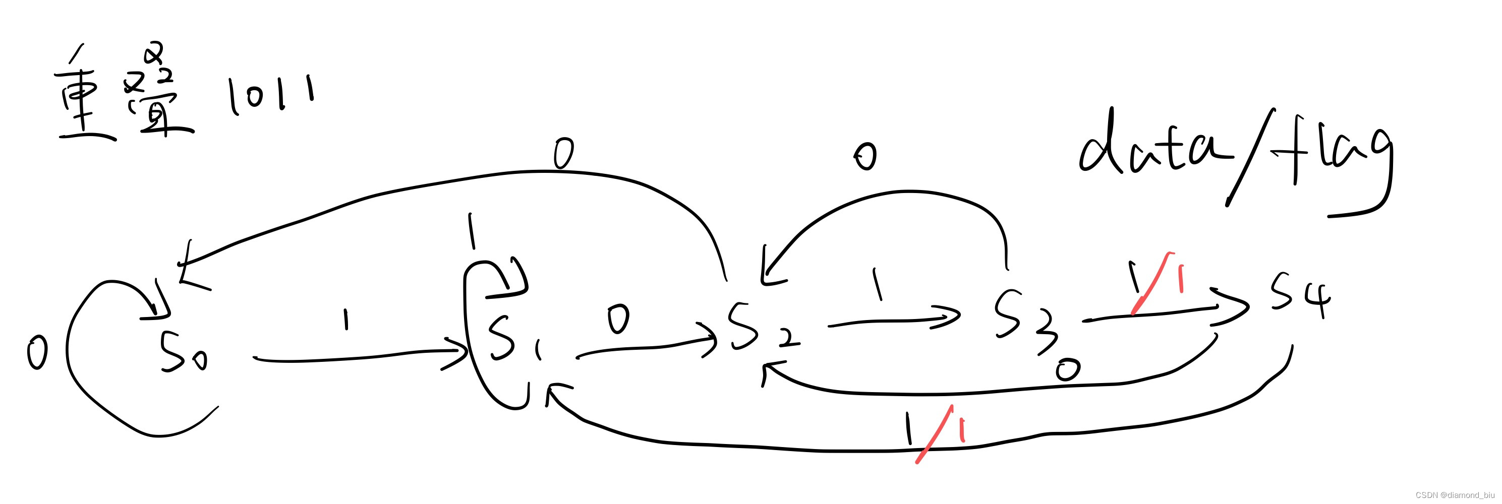
D<=~Q即可。`timescale 1ns/1ns
module even_div(
input wire rst ,
input wire clk_in,
output clk_out2,
output clk_out4,
output clk_out8
);
reg temp2,temp4,temp8;
always @ (posedge clk_in or negedge rst) begin
if(!rst) temp2<=0;
else temp2<=~temp2;
end
always @ (posedge clk_out2 or negedge rst) begin
if(!rst) temp4<=0;
else temp4<=~temp4;
end
always @ (posedge clk_out4 or negedge rst) begin
if(!rst) temp8<=0;
else temp8<=~temp8;
end
assign clk_out2=temp2;
assign clk_out4=temp4;
assign clk_out8=temp8;
endmodule
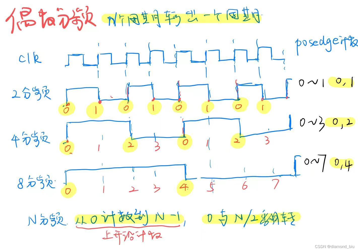
`timescale 1ns/1ns

module even_div(
    input     wire rst ,
    input     wire clk_in,
    output    reg clk_out2,
    output    reg clk_out4,
    output    reg clk_out8
    );

	reg count2;
	reg[1:0] count4;
	reg[2:0] count8;

	always @ (posedge clk_in or negedge rst) begin
		if(~rst) begin count2<=0;count4<=0;count8<=0;end
		else begin
			count2<=(count2==1)?0:count2+1;
			count4<=(count4==3)?0:count4+1;
			count8<=(count8==7)?0:count8+1;
		end
	end

	always @ (posedge clk_in or negedge rst) begin
		if(~rst) begin clk_out2<=0;clk_out4<=0;clk_out8<=0;end
		else begin
			clk_out2 <= (count2==0||count2==1) ? ~clk_out2 : clk_out2;
			clk_out4 <= (count4==0||count4==2) ? ~clk_out4 : clk_out4;
			clk_out8 <= (count8==0||count8==4) ? ~clk_out8 : clk_out8;
		end
	end
endmodule
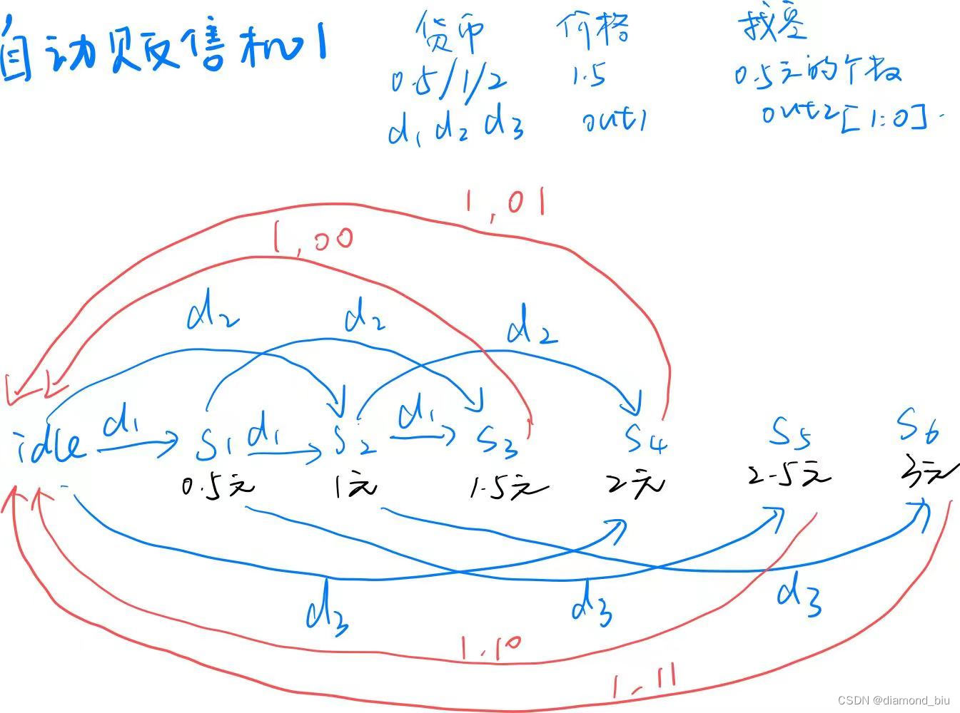
`timescale 1ns/1ns
module seller1(
	input wire clk  ,
	input wire rst  ,
	input wire d1 ,
	input wire d2 ,
	input wire d3 ,

	output reg out1,
	output reg [1:0]out2
	);
	reg[2:0] current_state,next_state;
	always @ (posedge clk or negedge rst) begin
		if(!rst) current_state<=0;
		else current_state<=next_state;
	end

	always@(*)begin
		if(!rst) next_state=0;
		else begin
			case(current_state)
			3'd0:next_state=d1 ? 3'd1 : d2 ? 3'd2 : d3 ? 3'd4 : next_state;
			3'd1:next_state=d1 ? 3'd2 : d2 ? 3'd3 : d3 ? 3'd5 : next_state;
			3'd2:next_state=d1 ? 3'd3 : d2 ? 3'd4 : d3 ? 3'd6 : next_state;
			default: next_state=3'd0;
			endcase
		end
	end

	always@(*)begin
		if(!rst) {out1,out2}=3'b0;
		else begin
			out1<=current_state==3'd3 || current_state==3'd4 || current_state==3'd5 || current_state==3'd6;
			out2<=current_state==3'd3 ? 2'b00 : current_state==3'd4 ? 2'b01 : current_state==3'd5 ? 2'b10 : current_state==3'd6 ? 2'b11 : 2'b00;
		end
	end

endmodule
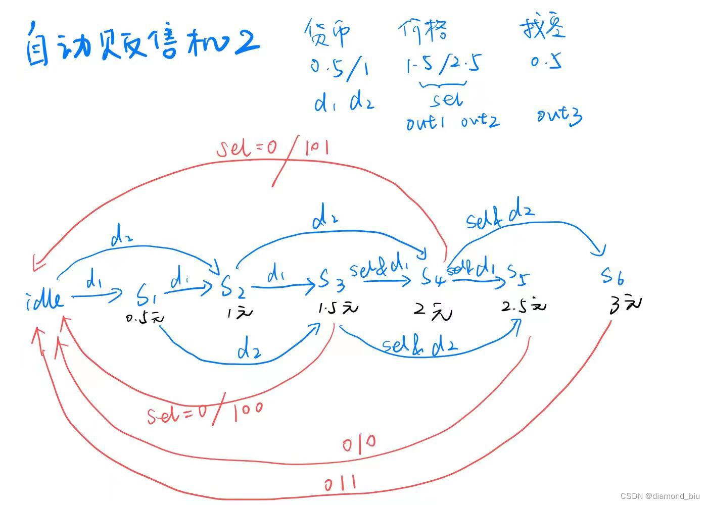
`timescale 1ns/1ns

module seller2(
	input wire clk  ,
	input wire rst  ,
	input wire d1 ,
	input wire d2 ,
	input wire sel ,

	output reg out1,
	output reg out2,
	output reg out3
	);
	reg[2:0] current_state,next_state;
	always @ (posedge clk or negedge rst) begin
		if(!rst) current_state<=0;
		else current_state<=next_state;
	end
	always @ (*) begin
		if(!rst) next_state=0;
		else begin
			case(current_state)
			3'd0:next_state=d1 ? 3'd1 : d2 ? 3'd2 : next_state;
			3'd1:next_state=d1 ? 3'd2 : d2 ? 3'd3 : next_state;
			3'd2:next_state=d1 ? 3'd3 : d2 ? 3'd4 : next_state;
			3'd3:next_state=sel ? (d1 ? 3'd4 : d2 ? 3'd5 : next_state) : 3'd0;
			3'd4:next_state=sel ? (d1 ? 3'd5 : d2 ? 3'd6 : next_state) : 3'd0;
			default:next_state=3'd0;
			endcase
		end
	end
	always @ (posedge clk or negedge rst) begin
		if(!rst) {out1,out2,out3}<=3'b000;
		else begin
			out1<=sel==0&&(next_state==3'd3 || next_state==3'd4 ) ;
			out2<=sel==1&&(next_state==3'd5 || next_state==3'd6 ) ;
			out3<=(sel==0&&next_state==3'd4) || (sel==1&&next_state==3'd6 ) ;
		end
	end
endmodule
clk_out=clk_p|clk_n;。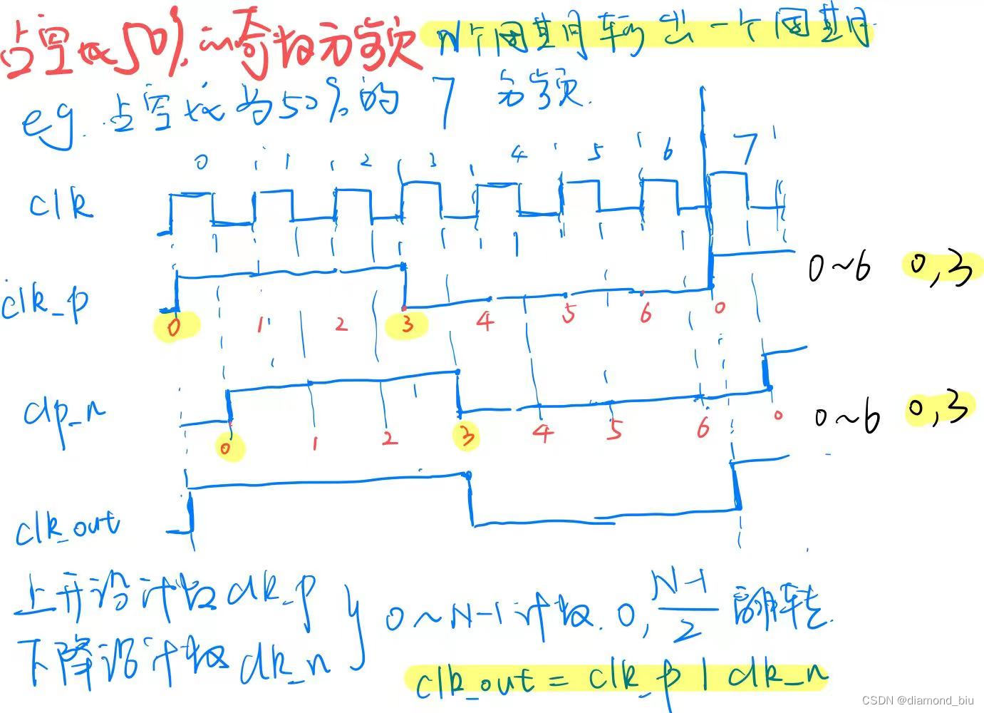
`timescale 1ns/1ns
module odo_div_or
   (
    input    wire  rst ,
    input    wire  clk_in,
    output   wire clk_out7
    );

	parameter N=7;
	reg[2:0] count_p,count_n;
	reg clk_p, clk_n;
	always @ (posedge clk_in or negedge rst) begin
		if(~rst) count_p<=0;
		else count_p<=(count_p==N-1)? 0 : count_p+1;
	end
	always @ (negedge clk_in or negedge rst) begin
		if(~rst) count_n<=0;
		else count_n<=(count_n==N-1)? 0 : count_n+1;
	end

	always @ (posedge clk_in or negedge rst) begin
		if(!rst) clk_p<=0;
		else clk_p<=(count_p==3||count_p==6) ? ~clk_p : clk_p;
	end
	always @ (negedge clk_in or negedge rst) begin
		if(!rst) clk_n<=0;
		else clk_n<=(count_n==3||count_n==6) ? ~clk_n : clk_n;
	end

	assign clk_out7=clk_p|clk_n;
endmodule
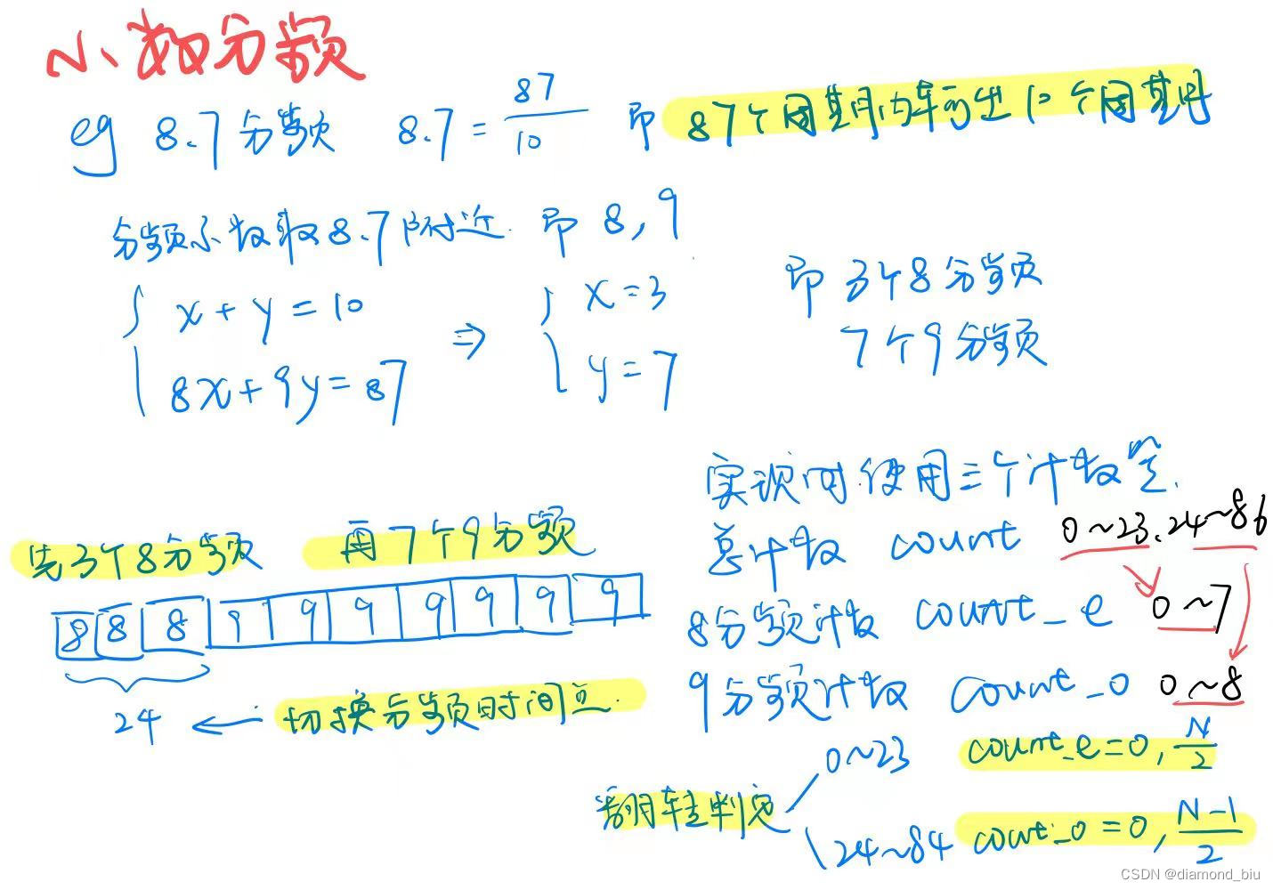
`timescale 1ns/1ns

module div_M_N(
 input  wire clk_in,
 input  wire rst,
 output wire clk_out
);
parameter M_N = 8'd87;
parameter c89 = 8'd24; // 8/9时钟切换点
parameter div_e = 5'd8; //偶数周期
parameter div_o = 5'd9; //奇数周期

reg [6:0]count;
reg [3:0] count_e;
reg [3:0] count_o;
reg clk_MN;
assign clk_out = clk_MN;

always @ (posedge clk_in or negedge rst) begin
    if(!rst) count<=0;
    else count<=(count==M_N-1) ? 0 : count+1;
end

always @ (posedge clk_in or negedge rst) begin
    if(!rst) count_e<=0;
    else count_e<=(count<=c89-1) ? (count_e==div_e-1 ? 0: count_e+1) : 0 ;
end
always @ (posedge clk_in or negedge rst) begin
    if(!rst) count_o<=0;
    else count_o<=(count>c89-1) ? (count_o==div_o-1 ? 0: count_o+1) : 0;
end

always @ (posedge clk_in or negedge rst) begin
    if(!rst) clk_MN<=0;
    else clk_MN<=(count<=c89-1)? (count_e==0||count_e==div_e/2 ? ~clk_MN : clk_MN) : (count_o==0||count_o==(div_o-1)/2 ? ~clk_MN : clk_MN);
end
endmodule
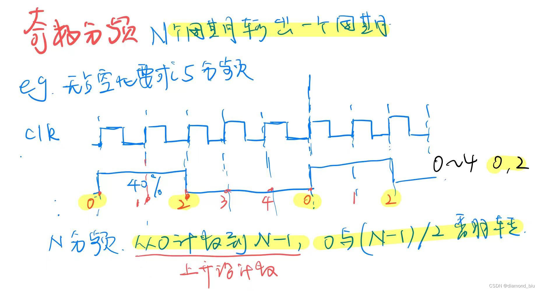
`timescale 1ns/1ns
module odd_div (
    input  wire rst ,
    input  wire clk_in,
    output reg clk_out5
	);
	parameter N=5;
	reg[2:0] count;

	always @ (posedge clk_in or negedge rst) begin
		if(!rst) count<=0;
		else count<=(count==N-1)? 0 : count+1;
	end
	always @ (posedge clk_in or negedge rst) begin
		if(!rst) clk_out5<=0;
		else clk_out5 <= (count==0||count==(N-1)/2) ? ~clk_out5 : clk_out5;
	end
endmodule
`timescale 1ns/1ns
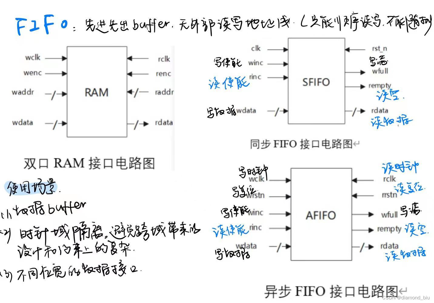
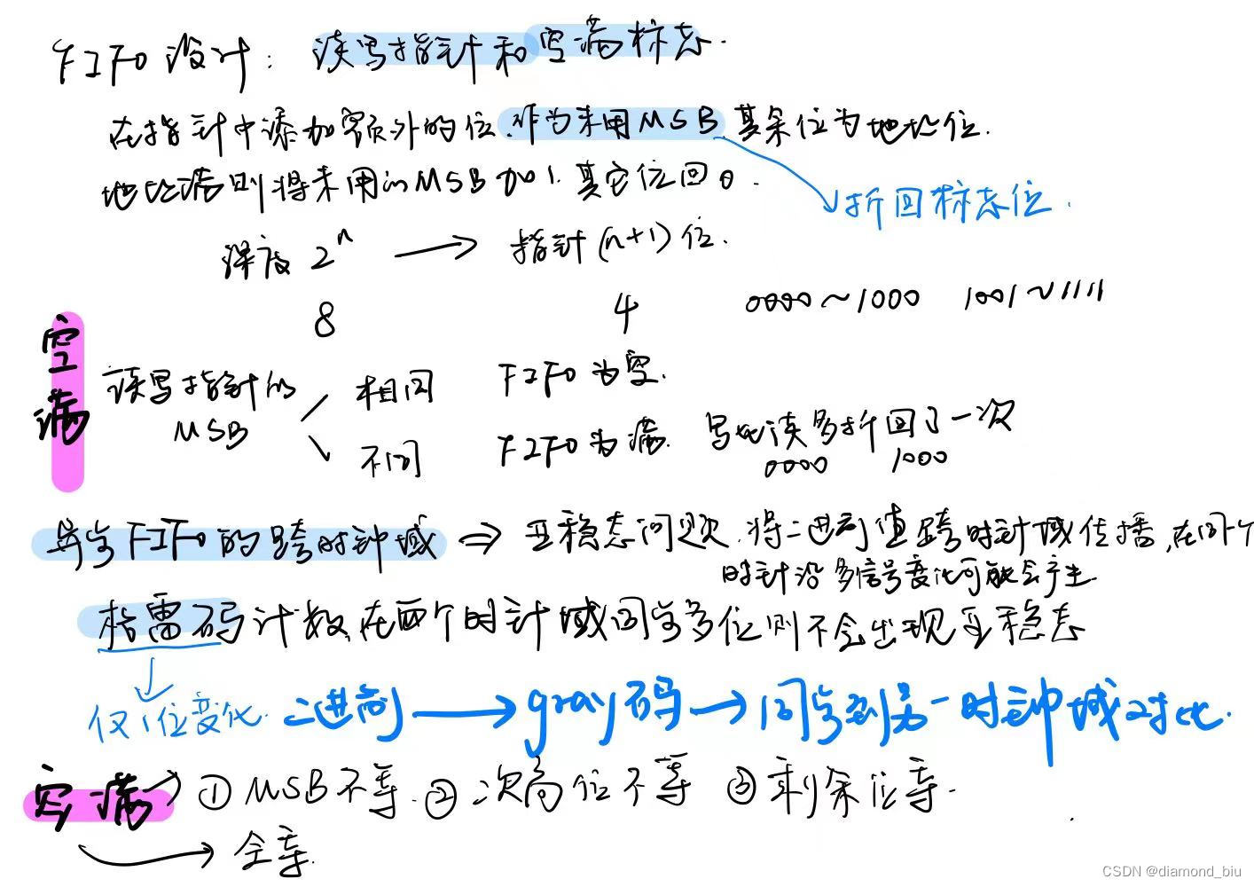
/***************************************RAM*****************************************/
module dual_port_RAM #(parameter DEPTH = 16,
parameter WIDTH = 8)(
input wclk
,input wenc
,input [$clog2(DEPTH)-1:0] waddr //深度对2取对数,得到地址的位宽。
,input [WIDTH-1:0] wdata //数据写入
,input rclk
,input renc
,input [$clog2(DEPTH)-1:0] raddr //深度对2取对数,得到地址的位宽。
,output reg [WIDTH-1:0] rdata //数据输出
);
reg [WIDTH-1:0] RAM_MEM [0:DEPTH-1];
always @(posedge wclk) begin
if(wenc)
RAM_MEM[waddr] <= wdata;
end
always @(posedge rclk) begin
if(renc)
rdata <= RAM_MEM[raddr];
end
endmodule
/***************************************AFIFO*****************************************/
module asyn_fifo#(
parameter WIDTH = 8,
parameter DEPTH = 16
)(
input wclk ,
input rclk ,
input wrstn ,
input rrstn ,
input winc ,
input rinc ,
input [WIDTH-1:0] wdata ,
output wire wfull ,
output wire rempty ,
output wire [WIDTH-1:0] rdata
);
reg [$clog2(DEPTH):0] waddr_bin,raddr_bin;
reg [$clog2(DEPTH):0] waddr_gray,raddr_gray,waddr_gray1,raddr_gray1,waddr_gray2,raddr_gray2;
wire wenc,renc;
// 读地址发生器
always @ (posedge rclk or negedge rrstn) begin
if(!rrstn) raddr_bin<=0;
else raddr_bin<=renc?raddr_bin+1:raddr_bin;
end
// 写地址发生器
always @ (posedge wclk or negedge wrstn) begin
if(!wrstn) waddr_bin<=0;
else waddr_bin<=wenc?waddr_bin+1:waddr_bin;
end
// 满信号发生器
assign wfull= (waddr_gray^raddr_gray2)==(2'b11<<($clog2(DEPTH)-1));
// 空信号发生器
assign rempty=raddr_gray==waddr_gray2;
// 格雷码产生与打拍
always @ (posedge rclk or negedge rrstn) begin
if(!rrstn) begin
raddr_gray<=0;waddr_gray1<=0;waddr_gray2<=0;
end
else begin
raddr_gray<=raddr_bin^(raddr_bin>>1);
waddr_gray1<=waddr_gray;
waddr_gray2<=waddr_gray1;
end
end
always @ (posedge wclk or negedge wrstn) begin
if(!wrstn) begin
waddr_gray<=0;raddr_gray1<=0;raddr_gray2<=0;
end
else begin
waddr_gray<=waddr_bin^(waddr_bin>>1);
raddr_gray1<=raddr_gray;
raddr_gray2<=raddr_gray1;
end
end
// RAM
assign wenc=winc&&!wfull;
assign renc=rinc&&!rempty;
dual_port_RAM #(
.DEPTH(DEPTH),
.WIDTH(WIDTH)
)
U1(
.wclk(wclk),
.wenc(wenc),
.waddr(waddr_bin[$clog2(DEPTH)-1:0]),
.wdata(wdata),
.rclk(rclk),
.renc(renc),
.raddr(raddr_bin[$clog2(DEPTH)-1:0]),
.rdata(rdata)
);
endmodule
`timescale 1ns/1ns
/**********************************RAM************************************/
module dual_port_RAM #(parameter DEPTH = 16,
parameter WIDTH = 8)(
input wclk
,input wenc
,input [$clog2(DEPTH)-1:0] waddr //深度对2取对数,得到地址的位宽。
,input [WIDTH-1:0] wdata //数据写入
,input rclk
,input renc
,input [$clog2(DEPTH)-1:0] raddr //深度对2取对数,得到地址的位宽。
,output reg [WIDTH-1:0] rdata //数据输出
);
reg [WIDTH-1:0] RAM_MEM [0:DEPTH-1];
always @(posedge wclk) begin
if(wenc)
RAM_MEM[waddr] <= wdata;
end
always @(posedge rclk) begin
if(renc)
rdata <= RAM_MEM[raddr];
end
endmodule
/**********************************SFIFO************************************/
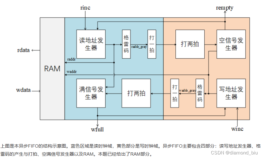
module sfifo#(
parameter WIDTH = 8,
parameter DEPTH = 16
)(
input clk ,
input rst_n ,
input winc ,
input rinc ,
input [WIDTH-1:0] wdata ,
output reg wfull ,
output reg rempty ,
output wire [WIDTH-1:0] rdata
);
reg [$clog2(DEPTH):0] waddr,raddr;
wire wenc,renc;
always @ (posedge clk or negedge rst_n) begin
if(!rst_n) begin
wfull<=0;rempty<=0;
end
else begin
wfull<=waddr==raddr+DEPTH;
rempty<=waddr==raddr;
end
end
assign wenc=winc&&!wfull;
assign renc=rinc&&!rempty;
always @ (posedge clk or negedge rst_n) begin
if(!rst_n) waddr<=0;
else waddr<=wenc ? waddr+1 : waddr;
end
always @ (posedge clk or negedge rst_n) begin
if(!rst_n) raddr<=0;
else raddr<=renc ? raddr+1 : raddr;
end
dual_port_RAM U1(
.wclk(clk),
.wenc(wenc),
.waddr(waddr),
.wdata(wdata),
.rclk(clk),
.renc(renc),
.raddr(raddr),
.rdata(rdata)
);
endmodule
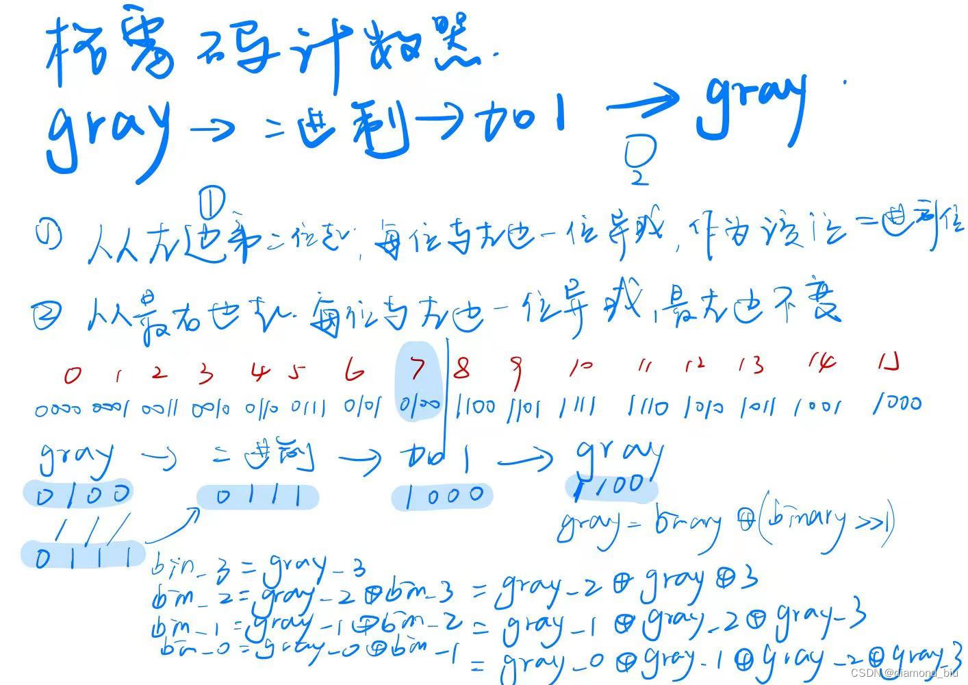
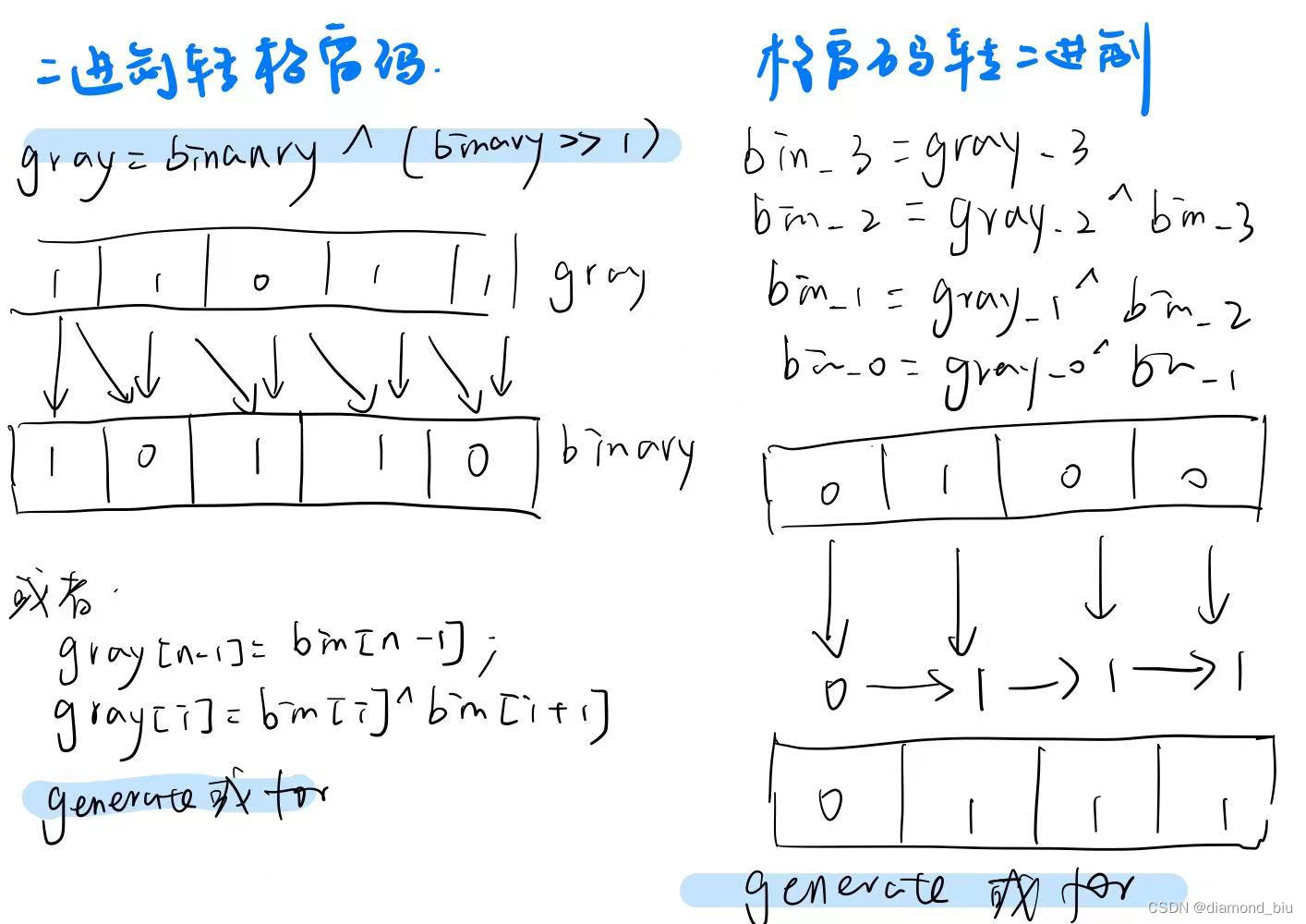
gray[n-1:0]来说,格雷码转二进制的方法是binary[n-1]=gray[n-1:0]; binary[i]=gray[i]^binary[i+1],i=n-2,...,1,0。对于二进制码binary_add[n-1:0]来说,二进制转格雷码的方法是gray=binary_add^(binary_add>>1);。`timescale 1ns/1ns
module gray_counter(
input clk,
input rst_n,
output reg [3:0] gray_out
);
wire[3:0] binary;
reg[3:0] binary_add;
//格雷码转二进制
assign binary={gray_out[3],gray_out[2]^gray_out[3],gray_out[1]^gray_out[2]^gray_out[3],gray_out[0]^gray_out[1]^gray_out[2]^gray_out[3]};
//二进制加一
always @ (posedge clk or negedge rst_n) begin
if(!rst_n) binary_add<=0;
else binary_add<=binary+1;
end
//二进制转格雷码
always @ (posedge clk or negedge rst_n) begin
if(!rst_n) gray_out<=0;
else gray_out<=binary_add^(binary_add>>1);
end
endmodule
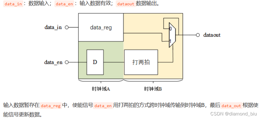
`timescale 1ns/1ns

module mux(
	input 				clk_a	,
	input 				clk_b	,
	input 				arstn	,
	input				brstn   ,
	input		[3:0]	data_in	,
	input               data_en ,

	output reg  [3:0] 	dataout
	);

	// 寄存输入数据
	reg [3:0] data_reg;
	always @ (posedge clk_a or negedge arstn) begin
		if(!arstn) data_reg<=0;
		else data_reg<=data_in;
	end

	//控制信号跨域打两拍
	reg data_en_a,data_en_b1,data_en_b2;
	always @ (posedge clk_a or negedge arstn) begin
		if(!arstn) data_en_a<=0;
		else data_en_a<=data_en;
	end
	always @ (posedge clk_b or negedge brstn) begin
		if(!brstn)  begin
			data_en_b1<=0;
			data_en_b2<=0;
		end
		else begin
			data_en_b1<=data_en_a;
			data_en_b2<=data_en_b1;
		end
	end

	// 同步到b时钟域的使能信号控制输出
	always @ (posedge clk_b or negedge brstn) begin
		if(!brstn) dataout<=0;
		else dataout<=data_en_b2?data_in:dataout;
	end

endmodule
`timescale 1ns/1ns

module pulse_detect(
	input 				clk_fast	,
	input 				clk_slow	,
	input 				rst_n		,
	input				data_in		,

	output  		 	dataout
	);
	reg data_level,data_level1,data_level2,data_level3;
	//脉冲转电平
	always @ (posedge clk_fast or negedge rst_n) begin
		if(!rst_n) data_level<=0;
		else data_level<=data_in ? ~data_level : data_level;
	end

	//电平信号打两拍再转脉冲
	always @ (posedge clk_slow or negedge rst_n) begin
		if(!rst_n) begin
			data_level1<=0;
			data_level2<=0;
			data_level3<=0;
		end
		else begin
			data_level1<=data_level;
			data_level2<=data_level1;
			data_level3<=data_level2;
		end
	end
	//异或表示两次都被采样到
	assign dataout=data_level2^data_level3;

endmodule
`timescale 1ns/1ns
module count_module(
	input clk,
	input rst_n,
    output reg [5:0]second,
    output reg [5:0]minute
	);

	always @ (posedge clk or negedge rst_n) begin
		if(!rst_n) second<=0;
		else second<=(second==60)? 1 : second+1;
	end

	always @ (posedge clk or negedge rst_n) begin
		if(!rst_n) minute<=0;
		else minute<=(second==60) ? (minute==60 ? minute : minute+1) : minute;
	end
endmodule
num暂存计数。`timescale 1ns/1ns
module count_module(
input clk,
input rst_n,
input set,
input [3:0] set_num,
output reg [3:0]number,
output reg zero
);
reg[3:0] num;
always @ (posedge clk or negedge rst_n) begin
if(!rst_n) num<=0;
else num<=set ? set_num : (num==15) ? 0 : num+1;
end
always @ (posedge clk or negedge rst_n) begin
if(!rst_n) number<=0;
else number<=num;
end
always @ (posedge clk or negedge rst_n) begin
if(!rst_n) zero<=0;
else zero<=num==0;
end
endmodule
`timescale 1ns/1ns

module count_module(
	input clk,
	input rst_n,
	input mode,
	output reg [3:0]number,
	output reg zero
	);
	reg[3:0] num;
	always @ (posedge clk or negedge rst_n) begin
		if(!rst_n) num<=0;
		else num<=mode ? (num==9 ? 0 : num+1) : (num==0 ? 9 : num-1);
	end

	always @ (posedge clk or negedge rst_n) begin
		if(!rst_n) number<=0;
		else number<=num;
	end

	always @ (posedge clk or negedge rst_n) begin
		if(!rst_n) zero<=0;
		else zero<=num==0;
	end
endmodule
`timescale 1ns/1ns

module RAM_1port(
    input clk,
    input rst,
    input enb,
    input [6:0]addr,
    input [3:0]w_data,
    output reg [3:0]r_data
	);
	parameter WIDTH = 4;
    parameter DEPTH = 128;
	reg[WIDTH-1:0] ram [DEPTH-1:0];
	integer i;
	always @ (posedge clk or negedge rst) begin
		if(~rst)begin
			for(i=0;i<DEPTH;i=i+1) ram[i]<=4'b0000;
		end
		else ram[addr]<=enb ? w_data : ram[addr];
	end
	always @ (*) begin
		if(!rst) r_data=0;
		else r_data=~enb ? ram[addr] : r_data;
	end
endmodule
`timescale 1ns/1ns
module ram_mod(
	input clk,
	input rst_n,

	input write_en,
	input [7:0]write_addr,
	input [3:0]write_data,

	input read_en,
	input [7:0]read_addr,
	output reg [3:0]read_data
	);
	parameter WIDTH = 4;
    parameter DEPTH = 8;
	reg[WIDTH-1:0] ram [DEPTH-1:0];

	integer i;
	always @ (posedge clk or negedge rst_n) begin
		if(~rst_n) begin
			for(i=0;i<DEPTH;i=i+1) ram[i]<=4'b0000;
		end
		else ram[write_addr]<=write_en ? write_data : ram[write_addr];
	end
	always @ (posedge clk or negedge rst_n) begin
		if(!rst_n) read_data<=0;
		else read_data<=read_en ? ram[read_addr] : 4'b0000;
	end

endmodule
略
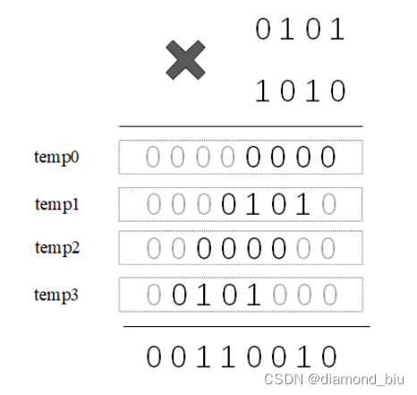
`timescale 1ns/1ns

module multi_pipe#(
	parameter size = 4
)(
	input 						clk 		,
	input 						rst_n		,
	input	[size-1:0]			mul_a		,
	input	[size-1:0]			mul_b		,

 	output	reg	[size*2-1:0]	mul_out
	);
	wire [size*2-1:0] temp [size-1:0];
	genvar i;
	generate
		for(i=0;i<size;i=i+1)begin:loop
			assign temp[i]=mul_b[i] ? mul_a<<i : 'd0;
		end
	endgenerate

	reg[size*2-1:0] adder_01,adder_23;
	always @ (posedge clk or negedge rst_n) begin
		if(!rst_n) adder_01<=0;
		else adder_01<=temp[0]+temp[1];
	end
	always @ (posedge clk or negedge rst_n) begin
		if(!rst_n) adder_23<=0;
		else adder_23<=temp[2]+temp[3];
	end
	always @ (posedge clk or negedge rst_n) begin
		if(!rst_n) mul_out<=0;
		else mul_out<=adder_01+adder_23;
	end
endmodule
`timescale 1ns/1ns

module triffic_light
    (
		input rst_n, //异位复位信号,低电平有效
        input clk, //时钟信号
        input pass_request,
		output wire[7:0]clock,
        output reg red,
		output reg yellow,
		output reg green
    );
	reg[1:0] current_state,next_state;
	reg[7:0] clock1;
	parameter idle=2'd0, s1=2'd1, s2=2'd2, s3=2'd3;
	always @ (posedge clk or negedge rst_n) begin
		if(!rst_n) current_state<=idle;
		else current_state<=next_state;
	end

	always@(*)begin
		if(!rst_n) next_state=idle;
		else begin
			case(current_state)
			idle:next_state=(clock1==8'd8) ? s1:idle;
			s1:next_state=(clock1==8'd1) ? s2:s1;
			s2:next_state=(clock1==8'd1) ? s3:s2;
			s3:next_state=(clock1==8'd1) ? s1:s3;
			endcase
		end
	end

	always @ (posedge clk or negedge rst_n) begin
		if(!rst_n) clock1<=8'd10;
		else begin
			case(current_state)
			idle:clock1<=(clock1==8'd8) ? 8'd10: clock1-1;
			s1:clock1<=(clock1==8'd1) ? 8'd5 : clock1-1;
			s2:clock1<=(clock1==8'd1) ? 8'd60 : clock1-1;
			s3:clock1<=(clock1>10 && pass_request) ? 8'd10 : (clock1==8'd1) ? 8'd10 : clock1-1;
			endcase
		end
	end


	always @ (posedge clk or negedge rst_n) begin
		if(!rst_n) {red,yellow,green}<=3'b000;
		else begin
			case(next_state)
			idle:{red,yellow,green}<=3'b000;
			s1:{red,yellow,green}<=3'b100;
			s2:{red,yellow,green}<=3'b010;
			s3:{red,yellow,green}<=3'b001;
			endcase
		end
	end

    assign clock=clock1;

endmodule
(remain<10 && remain>0),如果不限制remain>0,初始状态黄灯就会亮。`timescale 1ns/1ns
module game_count
(
input rst_n, //异位复位信号,低电平有效
input clk, //时钟信号
input [9:0]money,
input set,
input boost,
output reg[9:0]remain,
output reg yellow,
output reg red
);
always @ (posedge clk or negedge rst_n) begin
if(!rst_n) remain<=0;
else remain<=set ? remain+money : boost ? remain-2 : remain-1;
end
always @ (posedge clk or negedge rst_n) begin
if(!rst_n) yellow<=0;
else yellow<=(remain<10 && remain>0);
end
always @ (posedge clk or negedge rst_n) begin
if(!rst_n) red<=0;
else red<=(remain==0) || (remain==1&&boost==1);
end
endmodule
wire型的。`timescale 1ns/1ns
module RTL(
input clk,
input rst_n,
input data_in,
output data_out
);
wire data_in_q,data_out_q;
DFF U1(clk,rst_n,data_in,data_in_q);
DFF U2(clk,rst_n,~data_in_q&data_in,data_out);
endmodule
module DFF(
input clk,
input rst_n,
input D,
output reg Q
);
always @ (posedge clk or negedge rst_n) begin
if(!rst_n) Q<=0;
else Q<=D;
end
endmodule
`timescale 1ns/1ns

module sequence_generator(
	input clk,
	input rst_n,
	output reg data
	);
	reg[2:0] count;
	always@(posedge clk or negedge rst_n)begin
		if(!rst_n)count<=0;
		else count<=(count==3'd5)? 0 : count+1;
	end
	always@(posedge clk or negedge rst_n)begin
		if(!rst_n)data<=0;
		else data<=count==2||count==4||count==5;
	end
endmodule
`timescale 1ns/1ns
module huawei5(
	input wire clk  ,
	input wire rst  ,
	input wire [3:0]d ,
	output reg valid_in ,
	output wire dout
	);

//*************code***********//
reg [3:0] reg_d;
reg [1:0] count;

always @ (posedge clk or negedge rst) begin
    if(!rst) count<=0;
    else count<= count+1;
end

always @ (posedge clk or negedge rst) begin
    if(!rst) valid_in<=0;
    else valid_in<=(count==2'd3)? 1 : 0;
end

always @ (posedge clk or negedge rst) begin
    if(!rst) reg_d<=0;
    else reg_d<=(count==2'd3) ? d : reg_d<<1;
end

assign dout=reg_d[3];
endmodule
略
`timescale 1ns/1ns

/**********************************RAM************************************/
module dual_port_RAM #(parameter DEPTH = 16,
					   parameter WIDTH = 8)(
	 input wclk
	,input wenc
	,input [$clog2(DEPTH)-1:0] waddr
	,input [WIDTH-1:0] wdata
	,input rclk
	,input renc
	,input [$clog2(DEPTH)-1:0] raddr
	,output reg [WIDTH-1:0] rdata
);

reg [WIDTH-1:0] RAM_MEM [0:DEPTH-1];

always @(posedge wclk) begin
	if(wenc)
		RAM_MEM[waddr] <= wdata;
end

always @(posedge rclk) begin
	if(renc)
		rdata <= RAM_MEM[raddr];
end

endmodule

/**********************************SFIFO************************************/
module sfifo#(
	parameter	WIDTH = 8,
	parameter 	DEPTH = 16
)(
	input 					clk		,
	input 					rst_n	,
	input 					winc	,
	input 			 		rinc	,
	input 		[WIDTH-1:0]	wdata	,

	output reg				wfull	,
	output reg				rempty	,
	output wire [WIDTH-1:0]	rdata
);
reg[$clog2(DEPTH):0] waddr,raddr;
wire wenc,renc;

// 读写地址发生器
always @ (posedge clk or negedge rst_n) begin
    if(!rst_n)waddr<=0;
    else waddr<= wenc ? waddr+1 : waddr;
end
always @ (posedge clk or negedge rst_n) begin
    if(!rst_n)raddr<=0;
    else raddr<= renc ? raddr+1 : raddr;
end

// 空满信号发生器
always @ (posedge clk or negedge rst_n) begin
    if(!rst_n) begin
        wfull<=0;
		rempty<=0;
    end
    else begin
        wfull <= (waddr==raddr+DEPTH);
		rempty <= (waddr==raddr);
    end
end

// RAM
assign wenc=winc&!wfull;
assign renc=rinc&!rempty;

dual_port_RAM #(
	.DEPTH(DEPTH),
	.WIDTH(WIDTH)
	)
	U1(
	.wclk(clk),
	.wenc(wenc),
	.waddr(waddr[$clog2(DEPTH)-1:0]),
	.wdata(wdata),
	.rclk(clk),
	.renc(renc),
	.raddr(raddr[$clog2(DEPTH)-1:0]),
	.rdata(rdata)
	);
endmodule
clk_out=clk_p|clk_n;。`timescale 1ns/1ns
module clk_divider
#(parameter dividor = 5)
( input clk_in,
input rst_n,
output clk_out
);
reg clk_p,clk_n;
reg [$clog2(dividor):0] count;
always @ (posedge clk_in or negedge rst_n) begin
if(~rst_n) count<=0;
else count<=(count==dividor-1)? 0 : count+1;
end
always @ (posedge clk_in or negedge rst_n) begin
if(~rst_n) clk_p<=0;
else clk_p<=(count==(dividor-1)/2||count==dividor-1) ? ~clk_p : clk_p;
end
always @ (negedge clk_in or negedge rst_n) begin
if(~rst_n) clk_n<=0;
else clk_n<=(count==(dividor-1)/2||count==dividor-1) ? ~clk_n : clk_n;
end
assign clk_out=clk_p|clk_n;
endmodule
+优先级高于<<;`timescale 1ns/1ns
module calculation(
input clk,
input rst_n,
input [3:0] a,
input [3:0] b,
output reg[8:0] c
);
reg[8:0] temp;
always @ (posedge clk or negedge rst_n) begin
if(!rst_n) temp<=0;
else temp<=(a<<2) + (a<<3) + b + (b<<2);
end
always @ (posedge clk or negedge rst_n) begin
if(!rst_n) c<=0;
else c<=temp;
end
endmodule
给定这段代码defcreate@upgrades=User.update_all(["role=?","upgraded"],:id=>params[:upgrade])redirect_toadmin_upgrades_path,:notice=>"Successfullyupgradeduser."end我如何在该操作中实际验证它们是否已保存或未重定向到适当的页面和消息? 最佳答案 在Rails3中,update_all不返回任何有意义的信息,除了已更新的记录数(这可能取决于您的DBMS是否返回该信息)。http://ar.ru
如何在buildr项目中使用Ruby?我在很多不同的项目中使用过Ruby、JRuby、Java和Clojure。我目前正在使用我的标准Ruby开发一个模拟应用程序,我想尝试使用Clojure后端(我确实喜欢功能代码)以及JRubygui和测试套件。我还可以看到在未来的不同项目中使用Scala作为后端。我想我要为我的项目尝试一下buildr(http://buildr.apache.org/),但我注意到buildr似乎没有设置为在项目中使用JRuby代码本身!这看起来有点傻,因为该工具旨在统一通用的JVM语言并且是在ruby中构建的。除了将输出的jar包含在一个独特的、仅限ruby
在rails源中:https://github.com/rails/rails/blob/master/activesupport/lib/active_support/lazy_load_hooks.rb可以看到以下内容@load_hooks=Hash.new{|h,k|h[k]=[]}在IRB中,它只是初始化一个空哈希。和做有什么区别@load_hooks=Hash.new 最佳答案 查看rubydocumentationforHashnew→new_hashclicktotogglesourcenew(obj)→new_has
我将应用程序升级到Rails4,一切正常。我可以登录并转到我的编辑页面。也更新了观点。使用标准View时,用户会更新。但是当我添加例如字段:name时,它不会在表单中更新。使用devise3.1.1和gem'protected_attributes'我需要在设备或数据库上运行某种更新命令吗?我也搜索过这个地方,找到了许多不同的解决方案,但没有一个会更新我的用户字段。我没有添加任何自定义字段。 最佳答案 如果您想允许额外的参数,您可以在ApplicationController中使用beforefilter,因为Rails4将参数
我的主要目标是能够完全理解我正在使用的库/gem。我尝试在Github上从头到尾阅读源代码,但这真的很难。我认为更有趣、更温和的踏脚石就是在使用时阅读每个库/gem方法的源代码。例如,我想知道RubyonRails中的redirect_to方法是如何工作的:如何查找redirect_to方法的源代码?我知道在pry中我可以执行类似show-methodmethod的操作,但我如何才能对Rails框架中的方法执行此操作?您对我如何更好地理解Gem及其API有什么建议吗?仅仅阅读源代码似乎真的很难,尤其是对于框架。谢谢! 最佳答案 Ru
我的假设是moduleAmoduleBendend和moduleA::Bend是一样的。我能够从thisblog找到解决方案,thisSOthread和andthisSOthread.为什么以及什么时候应该更喜欢紧凑语法A::B而不是另一个,因为它显然有一个缺点?我有一种直觉,它可能与性能有关,因为在更多命名空间中查找常量需要更多计算。但是我无法通过对普通类进行基准测试来验证这一点。 最佳答案 这两种写作方法经常被混淆。首先要说的是,据我所知,没有可衡量的性能差异。(在下面的书面示例中不断查找)最明显的区别,可能也是最著名的,是你的
几个月前,我读了一篇关于rubygem的博客文章,它可以通过阅读代码本身来确定编程语言。对于我的生活,我不记得博客或gem的名称。谷歌搜索“ruby编程语言猜测”及其变体也无济于事。有人碰巧知道相关gem的名称吗? 最佳答案 是这个吗:http://github.com/chrislo/sourceclassifier/tree/master 关于ruby-寻找通过阅读代码确定编程语言的rubygem?,我们在StackOverflow上找到一个类似的问题:
我目前正在使用以下方法获取页面的源代码:Net::HTTP.get(URI.parse(page.url))我还想获取HTTP状态,而无需发出第二个请求。有没有办法用另一种方法做到这一点?我一直在查看文档,但似乎找不到我要找的东西。 最佳答案 在我看来,除非您需要一些真正的低级访问或控制,否则最好使用Ruby的内置Open::URI模块:require'open-uri'io=open('http://www.example.org/')#=>#body=io.read[0,50]#=>"["200","OK"]io.base_ur
前言作为一名程序员,自己的本质工作就是做程序开发,那么程序开发的时候最直接的体现就是代码,检验一个程序员技术水平的一个核心环节就是开发时候的代码能力。众所周知,程序开发的水平提升是一个循序渐进的过程,每一位程序员都是从“菜鸟”变成“大神”的,所以程序员在程序开发过程中的代码能力也是根据平时开发中的业务实践来积累和提升的。提高代码能力核心要素程序员要想提高自身代码能力,尤其是新晋程序员的代码能力有很大的提升空间的时候,需要针对性的去提高自己的代码能力。提高代码能力其实有几个比较关键的点,只要把握住这些方面,就能很好的、快速的提高自己的一部分代码能力。1、多去阅读开源项目,如有机会可以亲自参与开源
嗨~大家好,这里是可莉!今天给大家带来的是7个C语言的经典基础代码~那一起往下看下去把【程序一】打印100到200之间的素数#includeintmain(){ inti; for(i=100;i 【程序二】输出乘法口诀表#includeintmain(){inti;for(i=1;i 【程序三】判断1000年---2000年之间的闰年#includeintmain(){intyear;for(year=1000;year 【程序四】给定两个整形变量的值,将两个值的内容进行交换。这里提供两种方法来进行交换,第一种为创建临时变量来进行交换,第二种是不创建临时变量而直接进行交换。1.创建临时变量来